English
中国 China
Toggle navigation
Home
About PSD
Subscribe
Manage Subscription
Media Info
Join Newsletter
Glossary
Toggle navigation
Product News
Industry News
Departments
Design Tips
Dilbert
Distribution
Final Thought
MarketWatch
Notable & Newsworthy
Technical Features
TechTalk
ViewPoint
Design Centers
Automotive & Transportation
Batteries & Other Energy Storage Devices
Consumer
Data Centers
EV, Hybrids & Charging Infrastructure
Industrial
IoT & Smart Cities
Lighting & Illumination
Medical, Healthcare & Wellness
Military, Aerospace & Hi-Rel
Motor Drives, Robotics & Controls
Power Modules
Power Semiconductors
Power Supplies
Powering AI
Powering Communications
Powering Embedded Systems
Renewable Energy
Smart Power Grid
Test & Measurement
Wearables & Nanopower
White Goods
Wide-Bandgap Semis
PSDcast
PSDwebinar
Digital Magazines
Editor Blogs
Product News
Isolated DC-to-DC converters for Consumer, Industrial, and IoT Applications
Apr 18,2024
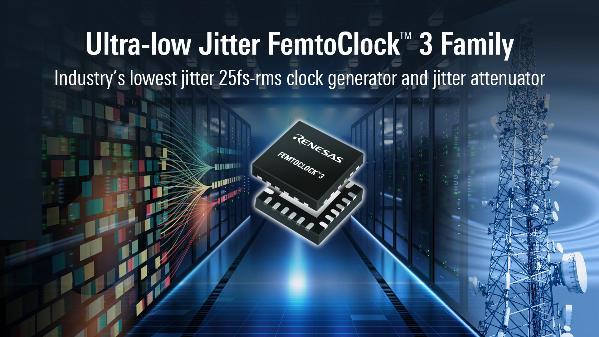
Renesas' New FemtoClock 3 Timing Solution Delivers Industry's Lowest Power and Leading Jitter Performance of 25fs-rms
Apr 18,2024
STMicroelectronics Extends Edge-AI Sensor Family With Inertial Module for Intensive Movement Analysis
Apr 18,2024
more
Industry News
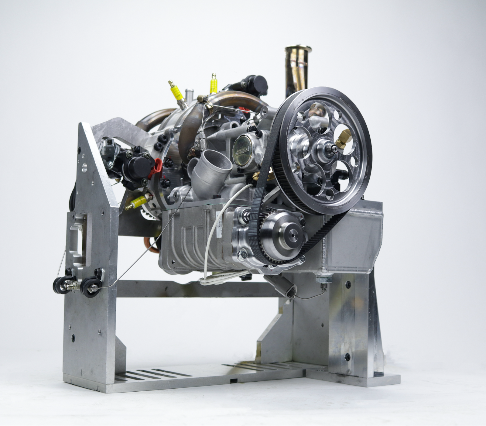
LiquidPiston Achieves Key Milestone for U.S. Army Development Program's 25hp Rotary Engine
Apr 18,2024
Navitas and Virtual Forest Join Hands to Advance Net-Zero in Agriculture
Apr 18,2024
New A.I. Project Will Allow Industrial Robots to be More Freethinking
Apr 17,2024
more
PSDcast
PSDcast – New Company to Help with Electric Transition
Apr 15,2024
PSDcast – Community Solar w/ Coach, Kate Spade, and Stuart Weitzman
Apr 11,2024
PSDcast – Advancing the Smart Home
Apr 3,2024
more
MarketWatch
Navigating the Industrial Electronics Market: Trends, Innovations and Growth Opportunities
Apr 1,2024
Analog Devices Expands Partnership with TSMC
Feb 26,2024
Power Supplies – Still Better to Buy
Mar 1,2024
more
Notable & Newsworthy
Isolated DC-to-DC converters for Consumer, Industrial, and IoT Applications
Apr 18,2024
Renesas' New FemtoClock 3 Timing Solution Delivers Industry's Lowest Power and Leading Jitter Performance of 25fs-rms
Apr 18,2024
LiquidPiston Achieves Key Milestone for U.S. Army Development Program's 25hp Rotary Engine
Apr 18,2024
more
Automotive & Transportation
Evolving EV Battery Technology Challenges Test Systems
Apr 16,2024
PSDcast – New Company to Help with Electric Transition
Apr 15,2024
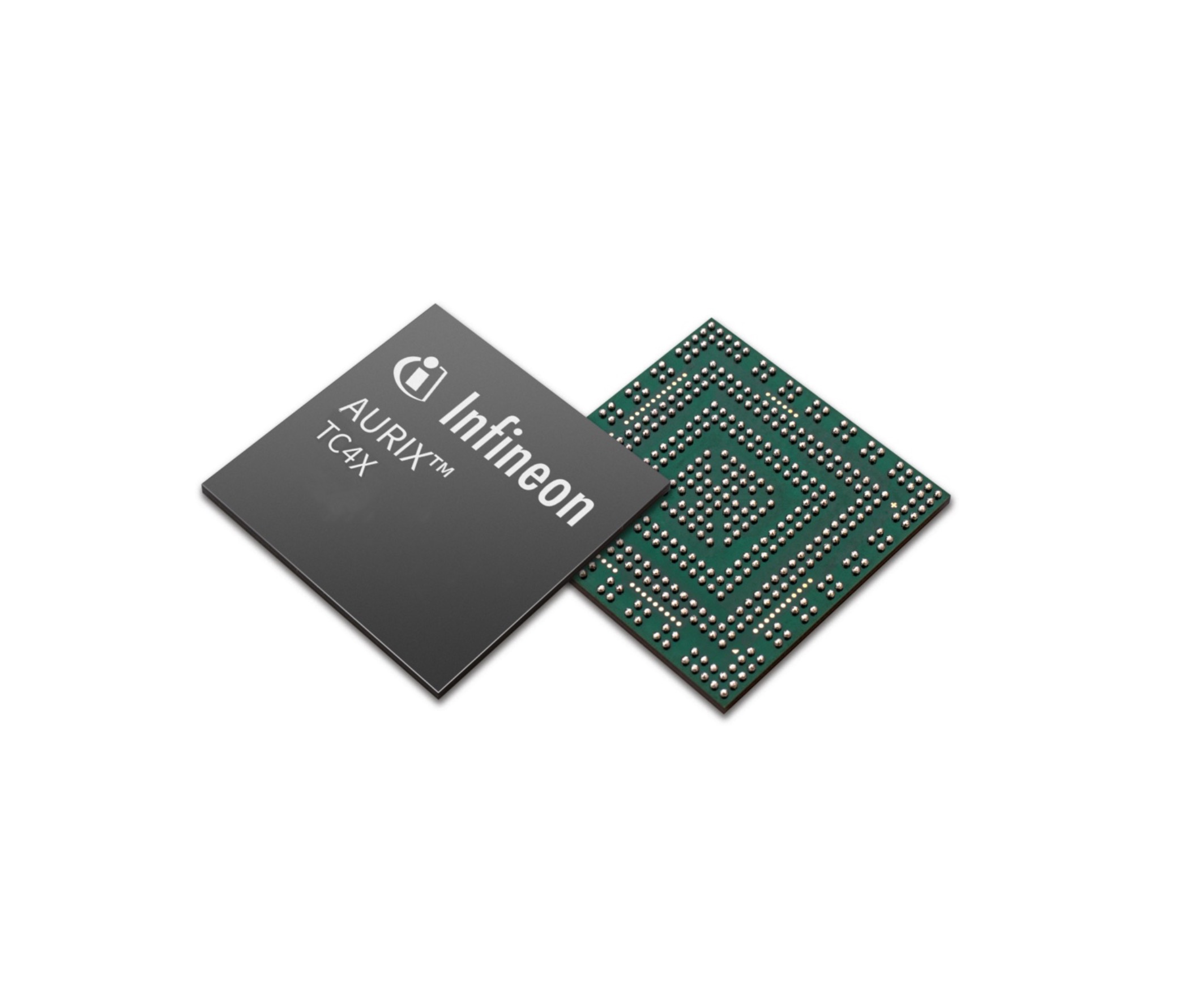
Vector Enables the Power of Infineon's AURIX TC4x Cyber Security Features
Apr 12,2024
more
Batteries & Other Energy Storage Devices
Better Batteries Require a Rethink
Apr 16,2024
Evolving EV Battery Technology Challenges Test Systems
Apr 16,2024
PSDcast – Community Solar w/ Coach, Kate Spade, and Stuart Weitzman
Apr 11,2024
more
Consumer
Isolated DC-to-DC converters for Consumer, Industrial, and IoT Applications
Apr 18,2024
STMicroelectronics Extends Edge-AI Sensor Family With Inertial Module for Intensive Movement Analysis
Apr 18,2024
Online 'Addiction' + Not Enough Sleep or Exercise Linked to Teen School Absence Risk
Apr 17,2024
more
Data Centers
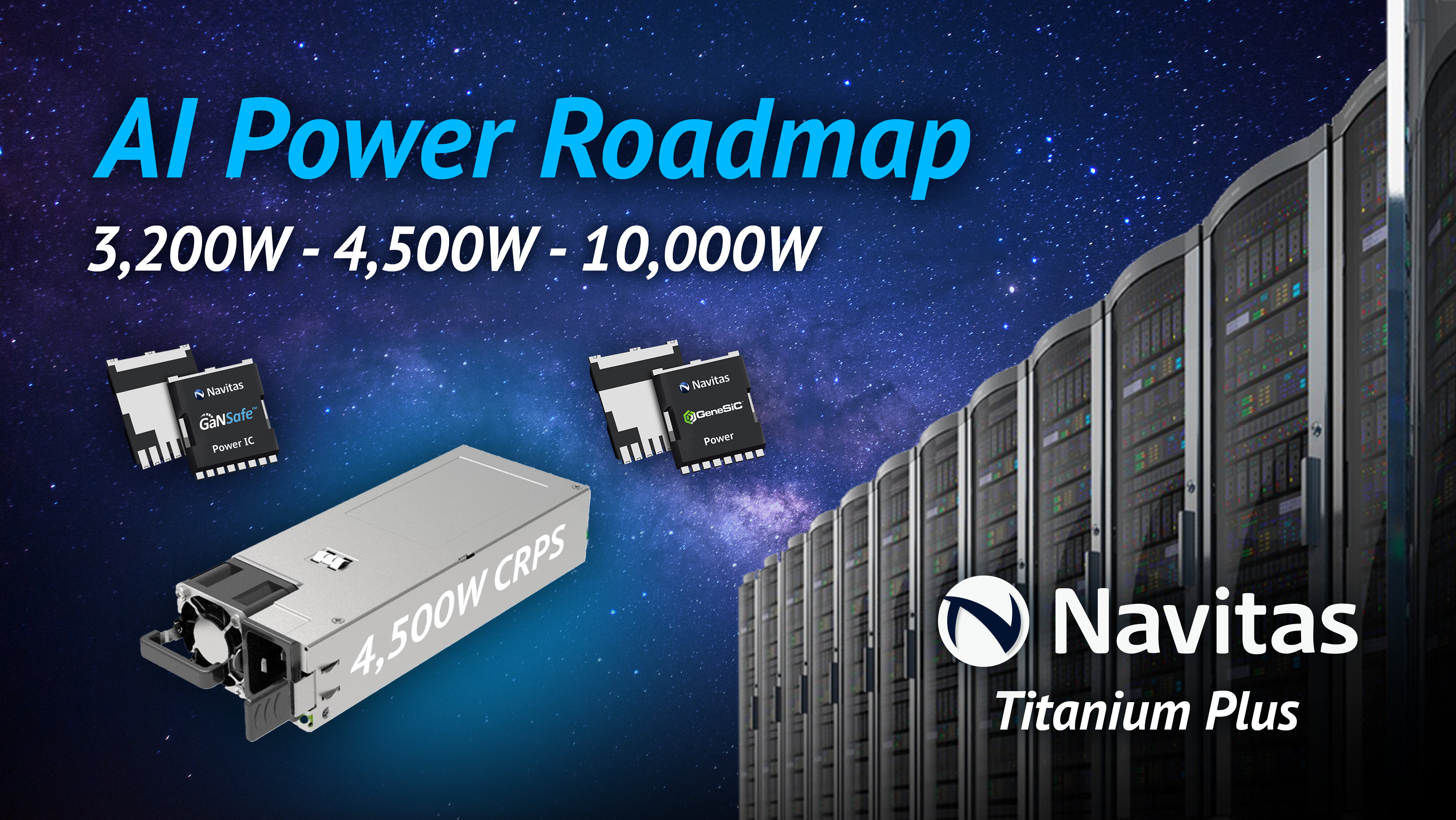
Navitas GaN and SiC Technologies to Enable Next-Gen AI Power Delivery
Mar 11,2024
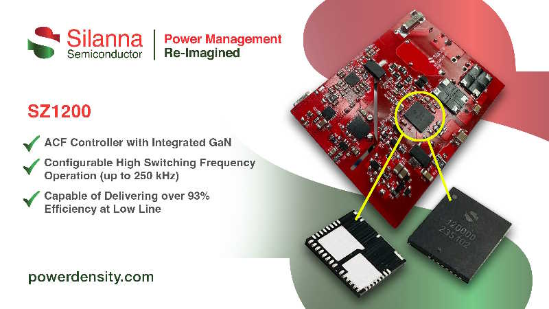
Silanna Semiconductor Takes ACF Integration to Next Level
Feb 26,2024
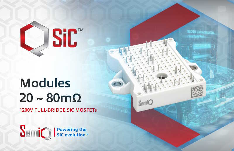
Efficient, Compact MOSFET Modules in Full-Bridge Configurations
Feb 26,2024
more
Powering Embedded Systems
TTI Europe Acquires Specialist Transportation Cable Assembly Manufacturer and Interconnect Distributor Raffenday Limited
Feb 21,2024
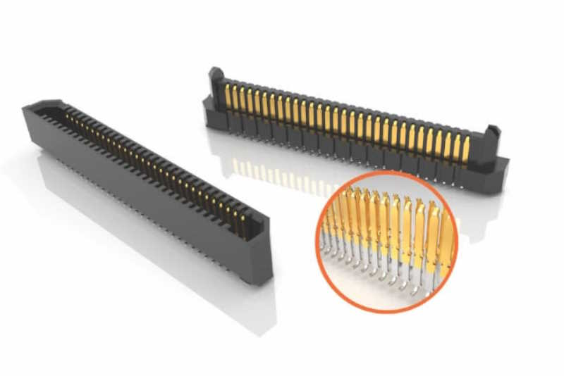
0.635 mm pitch, Slim Body Edge Rate Connectors
Feb 18,2024
Farnell Adds Murata’s Latest DC-DC Converters
Feb 18,2024
more
Industrial
Isolated DC-to-DC converters for Consumer, Industrial, and IoT Applications
Apr 18,2024
Renesas' New FemtoClock 3 Timing Solution Delivers Industry's Lowest Power and Leading Jitter Performance of 25fs-rms
Apr 18,2024
New A.I. Project Will Allow Industrial Robots to be More Freethinking
Apr 17,2024
more
Lighting & Illumination
Commercial Lighting Market Size is Expected to Reach USD 64.67 billion by 2031
Apr 4,2024
Würth Elektronik Presents LEDs with Integrated Controllers
Mar 27,2024
Angle-Dependent Holograms Made Possible by Metasurfaces
Mar 11,2024
more
Medical, Healthcare & Wellness
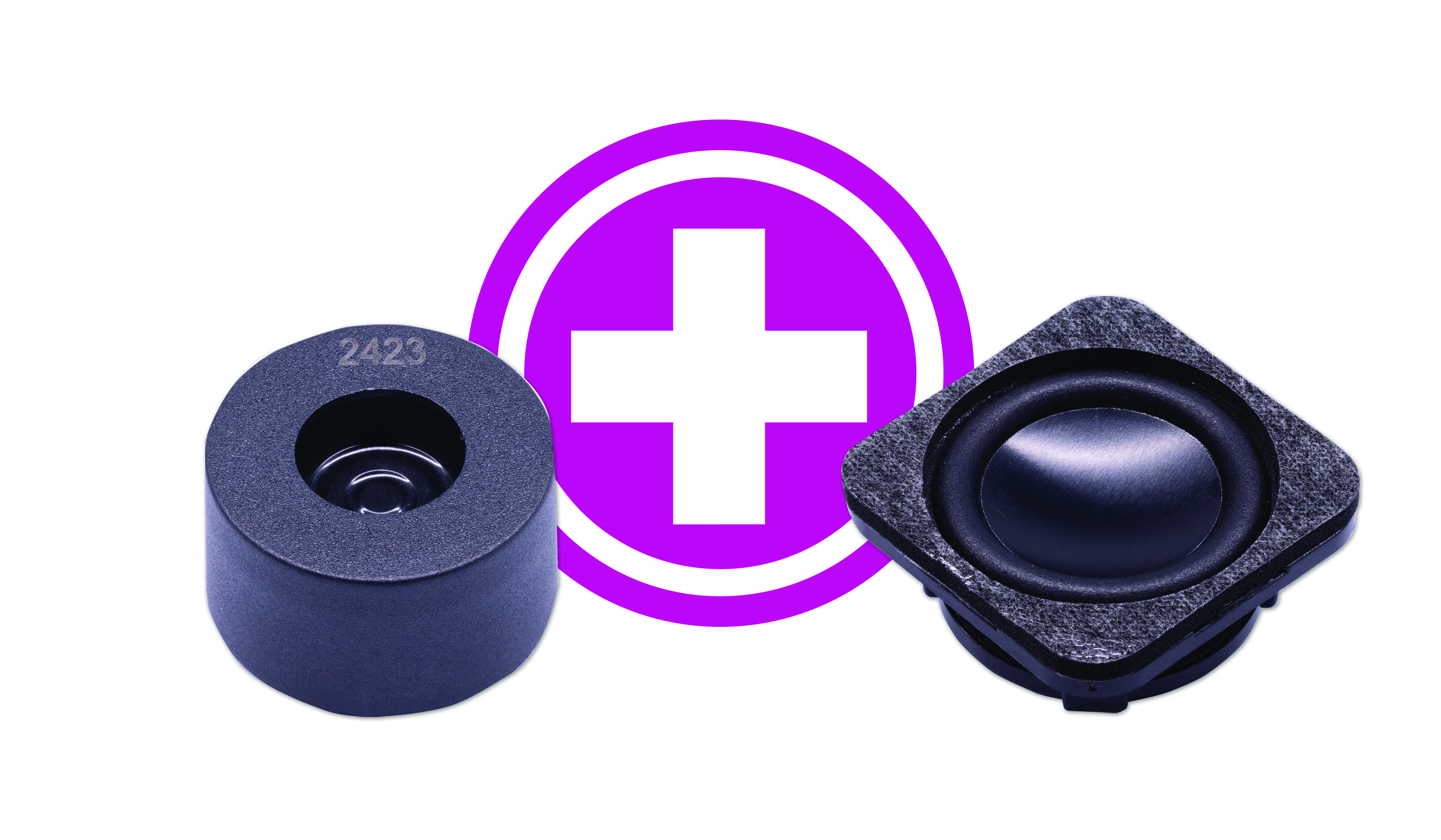
Medical Speakers Designed to Meet IEC 60601-1-8 Alarm Signal Requirements
Apr 2,2024
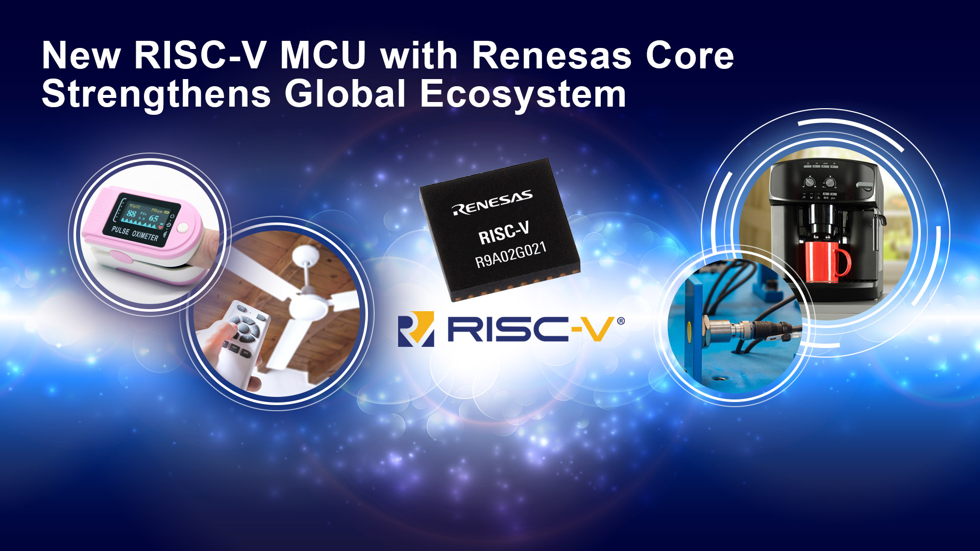
Renesas Introduces Industry's First General-Purpose 32-bit RISC-V MCUs with Internally Developed CPU Core
Mar 26,2024
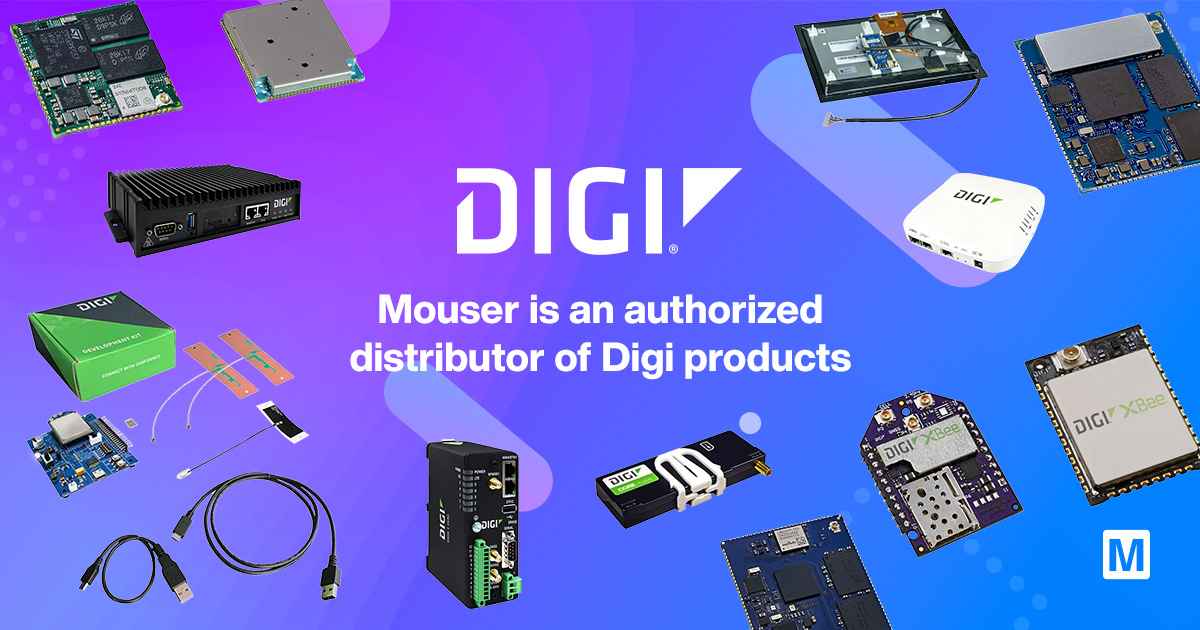
Mouser Electronics Stocking Newest Connectivity Solutions from Digi International Inc.
Mar 26,2024
more
Motor Drives, Robotics & Controls
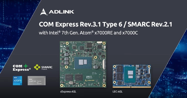
ADLINK Releases Intel Amston-Lake-powered Modules with up to 8 Cores at 12W TDP Suiting Ruggedized Edge Solutions
Apr 17,2024
RS Announces Three New Mechanical Power Transmission Solution Suppliers
Apr 10,2024
TDK Presents Enhanced Embedded Motor Controllers with Increased Memory, Power, and Reliability
Apr 4,2024
more
Powering Communications
STMicroelectronics Reveals New Family of 100V Trench Schottky Rectifier Diodes for Increased Efficiency and Power Density
Mar 26,2024
The Industry's First Wide Input Voltage Hot-Swap Controller for Telecom Infrastructure
Mar 21,2024
Finland Elevates High-Tech Profile with NATO Partnership, Establishing 6G Test Centre in Oulu
Mar 14,2024
more
Renewable Energy
Infinigen Renewables Announces Strategic Solar+ Battery Storage Project in Puerto Rico
Apr 17,2024
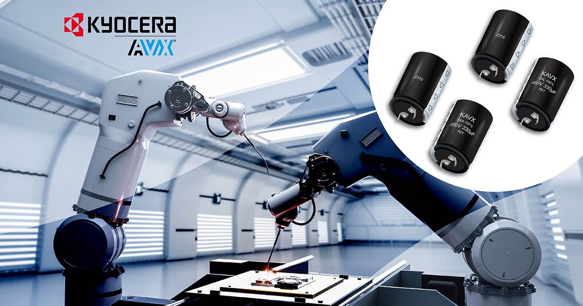
KYOCERA AVX Launches Two New Snap-In Aluminum Electrolytic Capacitor Series
Apr 17,2024
Wärtsilä Engines Again the Choice for Major Texas Utility Power Plant Project
Apr 17,2024
more
Smart Power Grid
PSDcast – Advancing the Smart Home
Apr 3,2024
PSDcast – Preventing Rolling Blackouts
Mar 15,2024
TTI Europe Acquires Specialist Transportation Cable Assembly Manufacturer and Interconnect Distributor Raffenday Limited
Feb 21,2024
more
Test & Measurement
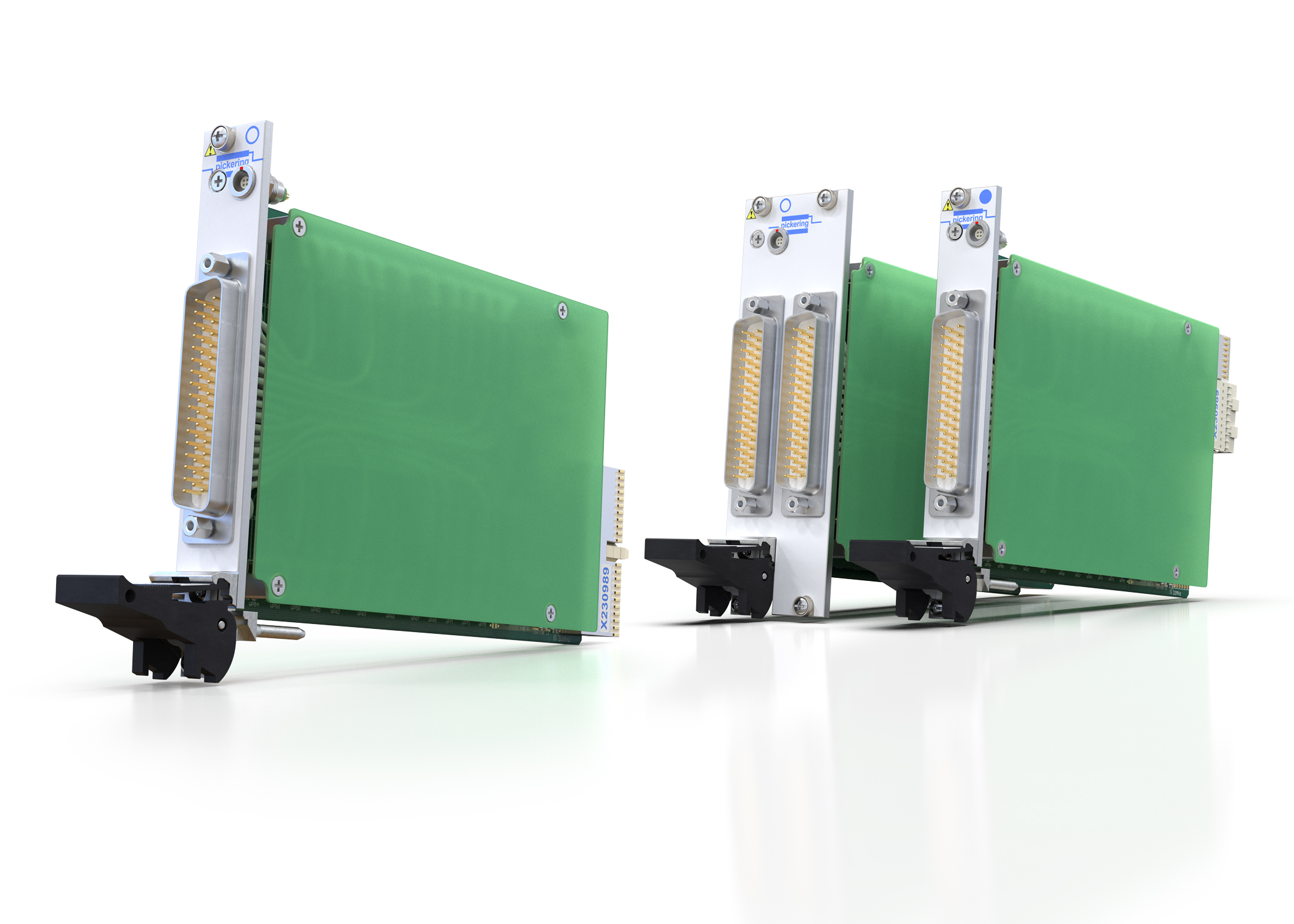
High-Voltage PXI Multiplexer Family from Pickering Interfaces Delivers Double the Switch Payload
Apr 11,2024
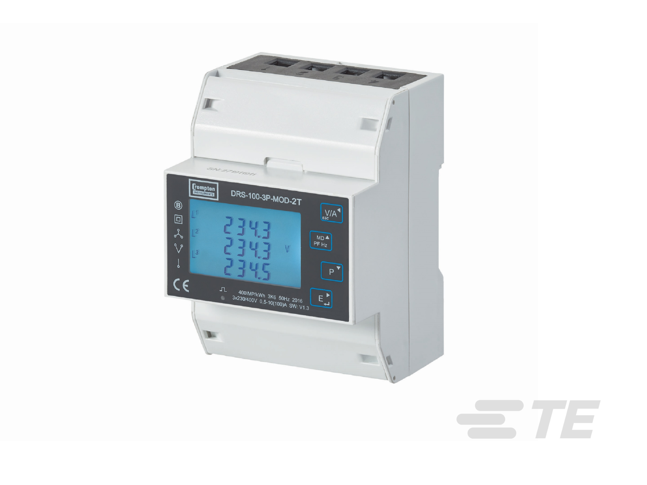
TTI Presents the DRS-100-3P MID Energy Meter from TE Connectivity
Mar 21,2024
SVS-Vistek Launches the World's Fastest High-Resolution SWIR Cameras for Industrial Imaging
Mar 18,2024
more
Technical Features
Evolving EV Battery Technology Challenges Test Systems
Apr 16,2024
DC/DC Flyback Converter
Apr 1,2024
Isolation Evolves to Keep Pace with Applications
Apr 1,2024
more
White Goods
Microchip Brings Enhanced Code Protection and up to 15W of Power Delivery to its USB Microcontroller Portfolio
Apr 10,2024
TTI Europe Acquires Specialist Transportation Cable Assembly Manufacturer and Interconnect Distributor Raffenday Limited
Feb 21,2024
0.635 mm pitch, Slim Body Edge Rate Connectors
Feb 18,2024
more
Dilbert
April 2024
March 2024
February 2024
more
×
Subscribe To Our PSDcast Channel
Please subscribe me to PSD's PSDcast Channel and keep me abreast of PSDcast activity
×
Please Add Your feedback/Rating for our PSDcast
Please click on stars to rate
Write Comments
Submit
×
Download Audio
Do you want to download
?
Home
|
Site Map
|
Contact
|
Privacy Policy
|
Refund Policy
|
Terms of Service
|
Copyright © 2024 Power Systems Design, All rights reserved
×
Join Our PSD's Daily Powersurge
Sign up Today for "Everything Power Electronics"
The Latest News and Exclusive Content from The Editors of PSD.
Select your Region
Europe
North America
China
Rest of Asia
South America
Other