A nanoscale rendering of the two materials, graphene (gray) and chromium oxide (blue). The red and green arrows represent spin.
The new design was developed by University of Nebraska–Lincoln’s Christian Binek and University at Buffalo’s Jonathan Bird and Keke He. Along with energy saving, the new design could cut the number of transistors needed to store certain types of data by up to 75%, leading to smaller devices. It is also non-volatile. By regulating the flow of current within an IC, the new transistor effectively acts as a nanoscopic on-off switch that’s essential to writing, reading and storing data.
“The traditional IC is facing some serious problems,” said Peter Dowben, Charles Bessey Professor of physics and astronomy at Nebraska and co-author of a recent paper on the work. “There is a limit to how much smaller it can get. We’re basically down to the range where we’re talking about 25 or fewer silicon atoms wide. And you generate heat with every device on an IC, so you can’t any longer carry away enough heat to make everything work, either.”
That predicament looms even as the demand for digital memory, and the energy needed to accommodate it, have soared.
In a transistor, the source and drain serve as the starting and end points for electrons flowing through. Above that channel sits the gate. Applying voltage between the gate and source can dictate whether the electric current flows with low or high resistance. Random-access memory requires a constant supply of power just to maintain those binary states.
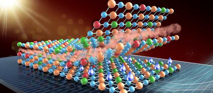
Rather than depend on electric charge as the basis of its approach, the team turned to spin - a magnetism-related property of electrons that points up or down and can be read, like electric charge can, as a 1 or 0. The team knew that electrons flowing through graphene, an ultra-robust material just one atom thick, can maintain their initial spin orientations for relatively long distances. Controlling the orientation of those spins, using substantially less power than a conventional transistor, was a much more challenging prospect.
To accomplish that, the researchers needed to underlay the graphene with chromium oxide. Chromium oxide is magneto-electric, meaning that the spins of the atoms at its surface can be flipped from up to down, or vice versa, by applying a small amount of temporary voltage. When applying positive voltage, the spins of the underlying chromium oxide point up, ultimately forcing the spin orientation of the graphene’s electric current to veer left and yield a detectable signal in the process. Negative voltage instead flips the spins of the chromium oxide down, with the spin orientation of the graphene’s current flipping to the right and generating a signal clearly distinguishable from the other. There are many alternatives to graphene that share its one-atom thickness but also boast properties better suited to a magneto-electric transistor. The race to overlay chromium oxide with those other 2D candidates is already on.
The team was supported by the National Science Foundation’s Established Program to Stimulate Competitive Research, which funded the $20 million Emergent Quantum Materials and Technologies collaboration at Nebraska, and from the Semiconductor Research Corporation.
 PDF
PDF