Author:
Randy Skinner, Staff Product Marketing Engineer, In-system programmable mixed signal products, Lattice Semiconductor Corp.
Date
02/03/2012
 PDF
PDF
Click image to enlarge
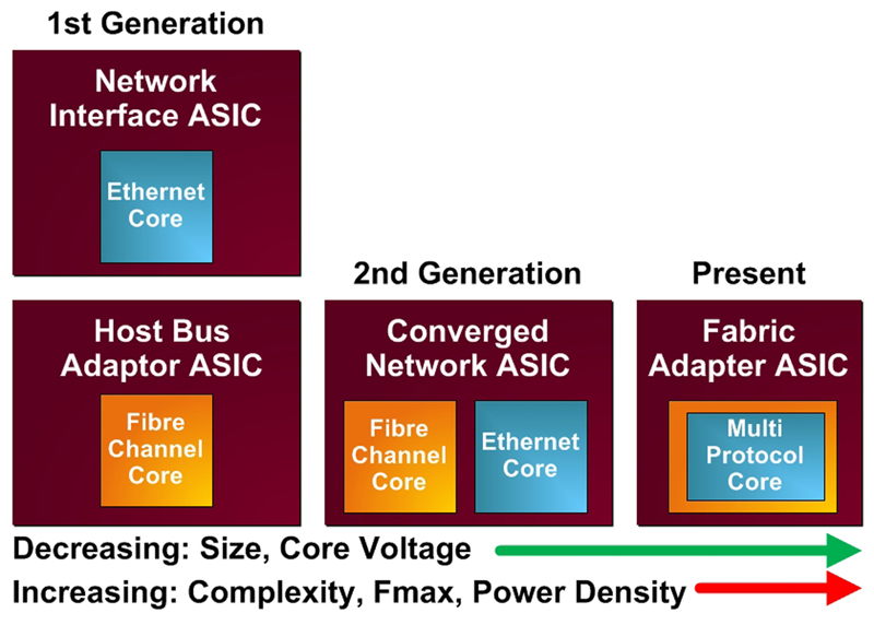
Figure 1: Development of Converged Network Adapter ASICs
Wouldn't it be nice to save 25% to 30%, or even more, in circuit board power dissipation in your next design? While for some designs such a savings would just be nice to have, for others it's a necessity to make the design competitive using the latest high performance integrated circuits. Why? Because the new ASICs, SoCs and processor technologies can be described in only one way -they are HOT! What led to this problem? The answer is increasing power density in IC technology. Even with shrinking transistor sizes and lower operational voltages, the number of transistors on a chip, and the frequency at which they switch, has increased at an even greater rate. The result is more power dissipated in a smaller area that ever before. Converged Network Adapter Evolution In the converged network adaptor market, integrated ASICs combine the functionality of a network interface card (NIC) with an Ethernet processing core and a host bus adapter (HBA) using Fiber Channel processing cores. Figure 1 traces the development of these highly adapted ASICs from separate functional ICs to devices with multiple core types on a single system on chip (SoC), to the present day Fabric Adapter ASIC capable of handling multiple protocols natively via a single IC core. This feat is accomplished with smaller process nodes and higher transistor counts than ever before possible. Multiple and lower operating voltages, along with higher clock switching speeds, facilitate this processing power in a smaller footprint than previously possible. While this advancement is exciting, there are limits to any technology, including these powerful new ASICs. Board designers who use these technology-enabling ICs now have more challenges than ever to deal with. In small, compact board area environments, the design challenges created by higher power densities include:
Power Management Strategy via Voltage Supply Scaling Using the example of the converged network adapter card, a new technique for lowering power dissipation is to lower the core operating voltage(s) of the ASIC in question. This is done while making sure manufacturer-specified operating conditions are maintained. The savings can be significant, as the power dissipated is a function primarily of the square of the operating voltage of the device. When load and digital processing conditions permit, the Vcore of the advanced ASIC can be reduced with power savings of 30% or more per IC. Those conditions include I/O loading, clock speed and other parameters such as temperature and operational characteristics. At appropriate times a circuit designed to control the setting of the Vcore of the ASIC can change the Vout of the supply delivering that voltage. In Figure 2 a dedicated MCU communicates with the ASIC and by implementing a closed-loop trimming algorithm adjusts the Vcore DC-DC converter in real time. The MCU measures Vcore from the DC-DC and then sends digital correction signals to the DC-DC via a voltage generated with an external digital-to-analog converter (DAC).
Challenges of Traditional Voltage Scaling Methods One of the challenges of implementing a working solution for setting the Vcore power supply to multiple values is the need for multiple external components in a closed loop control configuration. The measurement of the power supply output voltage is subject to the accumulation of errors created by ground potential variations and single-end voltage measurement techniques. Another disadvantage of single-end measurement is that it is not immune to noise. Traditional single end measurement is a poor alternative to differential input sensing and results in accuracies no better than 1.5% error (min). Other MCU-based solution challenges include the need for an external watchdog timer to insure that a hung processor condition does not occur. Finally, a custom-built solution is the most expensive alternative, especially when a large number of discrete ICs are required. Another item often overlooked is the risk and complexity of the stable closed loop trimming algorithm itself. A hung MCU or over-ranged ADC or DAC condition will result in unpredictable operation. Being too conservative and missing specification values will reduce power savings. A Complete Power Management Solution In addition to accurately scaling Vcore for multiple operating values, a complete board management solution should offer all of the following features: