Author:
Nancy Xiong, Maxim Integrated
Date
10/04/2013
 PDF
PDF

Click image to enlarge
Figure 1. Data from the MAX8805W show how a bypass FET affects output voltage line regulation.
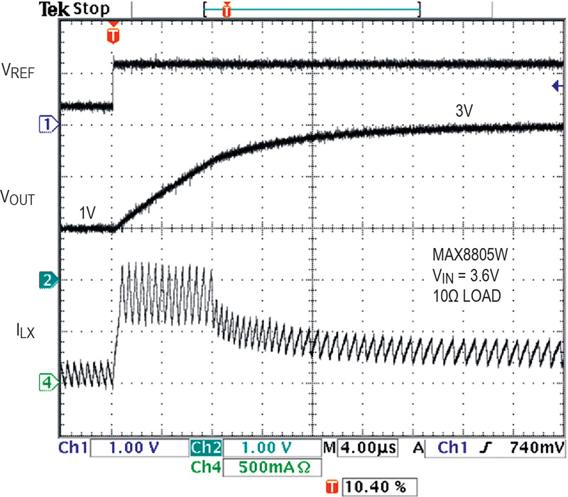
A hysteretic DC-DC step-down converter has been widely used in 2G/3G/4G RF power amplifiers (PAs) as a replacement for a direct battery supply to the PA's DC supply. By dynamically adjusting the PA supply voltage and bias current, this approach dramatically improves PA efficiency and extends battery life. A bypass mode with bypass FET or bypass LDO also reduces the dropout voltages across the step-down converter and enhances the output current capability. Together, these functions lower the battery shutdown point and extend battery life. The increased system efficiency by using a hysteretic step-down converter does, admittedly, involve a trade-off in voltage headroom. This article discusses how a bypass mode with a bypass FET or bypass LDO can be integrated into the hysteretic step-down converters to optimize PA performance. Basics of a hysteretic step-down converter A PA step-down converter differs from a traditional step-down converter that powers a digital processor core in several important ways. The PA converter offers dynamic output-voltage control for continuous PA power adjustment; high efficiency over a wide output voltage/current range; a fast turn-on time and settling time for output voltage change; low dropout and 100% duty cycle operation; and low output-voltage ripple. Modern hysteretic step-down converters dynamically control the DC supply voltage to the PA. The converter output voltage is adjusted by an independent DAC-controlled analog input in proportion to different RF transmitting power levels. The converter uses output voltage ripple to control when the high-side and low-side switches are turned on and off. It uses an error comparator without a fixed-frequency clock instead of an error amplifier with compensation. Therefore, the hysteretic converter's key significant advantage over a fixed-frequency PWM converter is its major improvement in transient response. Unlike a fixed-frequency converter, the hysteretic converter reacts immediately to any output voltage/load transient without having to wait for a new clock pulse or for the error amplifier output to move. With high efficiency, high switching frequency, and a 100% duty cycle, the hysteretic converter is a perfect candidate to power the PA. The importance of a bypass mode Using a hysteretic step-down converter instead of the battery itself to bias the PA does, admittedly, raise one issue: the efficiency improvement sacrifices voltage headroom. Inserting the converter between the battery and PA usually removes at least 200mV or more of headroom. Let's look at an example, the MAX8989 hysteretic step-down converter. To transmit 32dBm RF power on a certain PA module, the recommended VCC and ICC are 3.4V and 1130mA, respectively. Assume that the MAX8989 internal p-FET on-resistance (RON) is 175m? and that the inductor used has 200m? DCR. Then the total voltage drop across the p-FET and inductor is: (175m? + 200m?) × 1.13A = 424mV To sustain a 3.4V VCC voltage, the battery voltage must be above 3.824V, which shortens talk time. To overcome this issue, a bypass mode is implemented. Essential components of this bypass mode are the bypass FET and bypass LDO, and we will examine each in turn. Use a bypass FET to lower the dropout voltage The MAX8805W hysteretic step-down converter has a bypass mode with bypass FET. As the battery voltage drops and the converter approaches dropout region, its internal bypass FET connects the PA directly to the battery when VREFIN > 0.372 × VIN. Figure 1 demonstrates the performance difference when the bypass is enabled or disabled. Without the bypass FET, the dropout voltage after the converter enters 100% duty cycle is: VDROPOUT = (RON-PFET + DCRIND) × IOUT With the bypass FET on, the dropout voltage becomes: VDROPOUT = (RON-BYP//(RON-PFET + DCRIND)) × IOUT w Where RON-PFET is 180m? and RON-BYP is only 60m?. Using a 3.4V battery voltage, the MAX8805W's output voltage is 3.23V without the bypass FET on, and 3.37V with the bypass FET on. The bypass FET thus improves 140mV voltage headroom by lowering the dropout voltage. The bypass FET increases the converter's output to battery voltage in the dropout region. The trade-off is a voltage jump at the transition from the regulation region to the dropout region instead of the smooth transition shown in Figure 1. To obtain a smooth transition from the regulation region to the dropout region, a low-dropout linear regulator (a bypass LDO) in parallel with the step-down converter is introduced into hysteretic converters.
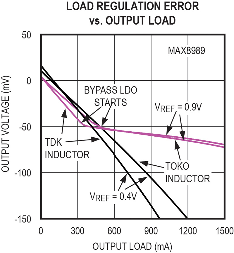
Use a bypass LDO to remove voltage "jump" Figure 1 also shows the improvement of a bypass LED over a bypass FET. This LDO provides a smooth transition between step-down regulation and operation in dropout. Two bypass LDO examples are presented using the MAX8989 and MAX8951. We start by looking at the MAX8989, where the relation between the output voltage and REFIN voltage is: VOUT = 2 × VREFIN - 0.5 × DCRIND × IOUT When the MAX8989 output voltage drops by more than 50mV due to load regulation (0.5 × DCRIND × IOUT > 50mV) and the output voltage is above the linear bypass enable threshold (1.4V, typ), the bypass LDO supplies supplementary current to the output to keep the output voltage in regulation. Figure 2 illustrates the effect of the bypass LDO on output voltage regulation. Here, the bypass LDO is disabled in the case of VREFIN = 0.4V; for VREFIN = 0.9V, the bypass LDO begins operation when the output voltage drops 50mV and the load regulation ramps down at a slower rate. Two inductors (a TOKO® DFE252012C-4R7 and a TDK® VLS252015ET-4R7M) are used and noted in Figure 2. With different inductors, the bypass LDO starts at the same 50mV point. But since the TDK inductor has bigger DCR and causes a higher voltage drop across the inductor, the bypass LDO begins operation at a lower output current. When the output current exceeds the step-down converter's current limit, the bypass LDO provides supplementary current to the output, thereby ensuring a stable output voltage. The bypass LDO does not provide any supply current before the step-down converter gets to its current limit. While the linear bypass regulator is sourcing current, the step-down converter continues to supply most of the load to maximize efficiency.
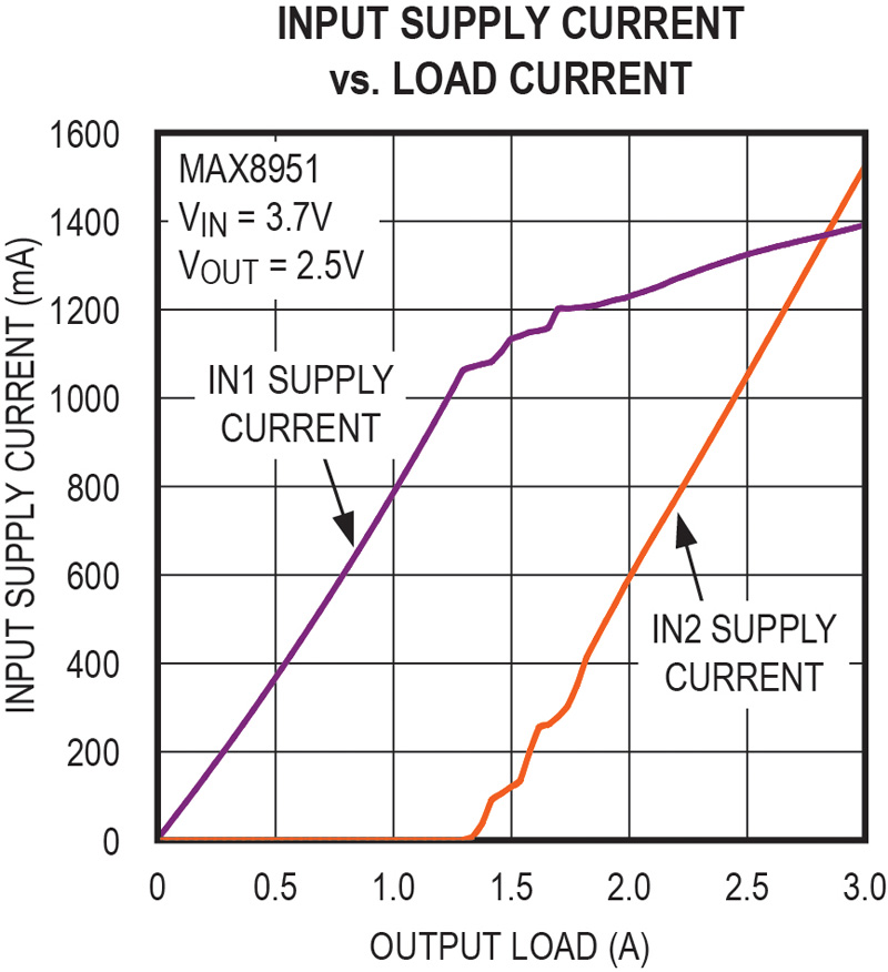
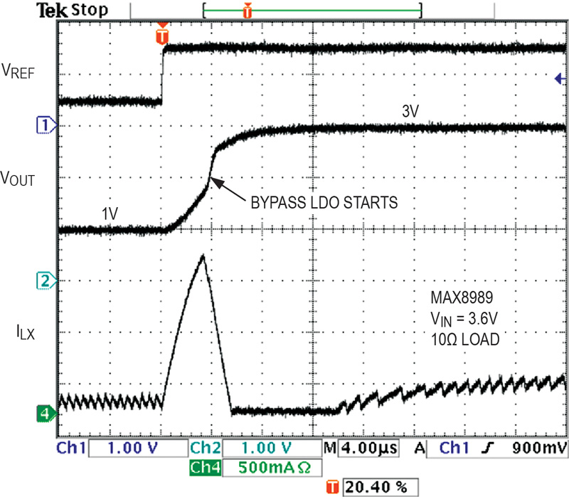
The MA8951 has separate input supplies for the hysteretic step-down converter (IN1) and bypass LDO (IN2). Figure 3 illustrates the IN1/IN2 supply-current delivery versus output load. The converter reaches its current limit at 1.3A load. Above a 1.3A load, the IN2 supply picks up the load and provides the supplemental current to the output. Therefore, with a bypass LDO, the inductor with a lower saturation current rating can be used in higher-current PA applications. A bypass LDO also enables a faster output voltage-transient response. Using the same setup for the MAX8989 described above, tests are done by stepping the REFIN voltage to get a 1V to 3V output voltage change. After the output voltage rises above the bypass-enable threshold, the bypass LDO starts and ramps up the output voltage at a faster rate. The MAX8989's overall settling time from 1V to 3V is less than 8μs, while this time for the MAX8805W is more than 16μs. Compare Figure 4 and Figure 5 for the devices' difference in output voltage-transient response.
Conclusion Hysteretic step-down converters with either a bypass FET or bypass LDO both optimize the PA performance and improve the system efficiency which extends battery life. A bypass LDO offers advantages over a bypass FET, specifically a smoother transition between step-down regulation and dropout and a faster transient response. These performance benefits make a step-down converter with a bypass LDO an ideal candidate for PA power applications. Maxim Integrated