Author:
Kazuyuki Fujii and Masahiro Okazaki, Torex Semiconductor
Date
10/30/2016
 PDF
PDF
Recently there have been efforts to lower below 1V the core voltage of various chipsets used for wearable devices and GPS/communication modules. This is due to the fact that holding down the core operating voltage enables a significant reduction of power consumption. Here we’ll go over a new ultra-low power DC-DC converter that can take full advantage of the “low power benefits” of these low-voltage chipsets.
The demand for low power consumption is growing in battery-driven devices such as wearable devices and mobile devices, and in energy harvest (environmental power) devices that do not have batteries. Various initiatives are being advanced to introduce low-power technology that maximizes the operating time of limited battery capacities and limited electrical energy.
Low-voltage core operation extends battery life
One reason for this is the lowered core voltage of chipsets incorporated in battery driven / energy harvesting devices. A lower voltage enables heightening of chipset processing performance without an increase of power consumption, or the same performance with reduced power consumption. For example, a chipset with a 1.8V core voltage can be simply replaced with a 0.7V core voltage chipset to extend battery life by about 2.5 times with the same performance and battery capacity. This is a tremendous benefit for wearable devices, whose spread has been hampered by “short battery life”.
Previously the chipset core of microcontrollers incorporated in wearable devices and GPS/Bluetooth modules incorporated in mobile devices most often operated at a voltage from 1.1 to 1.8V. Now efforts are being mode to reduce the core voltage to 0.6 to 0.8V, and chipsets with a core that operates at an ultralow voltage of 1V or less are starting to appear (see Figure 1).
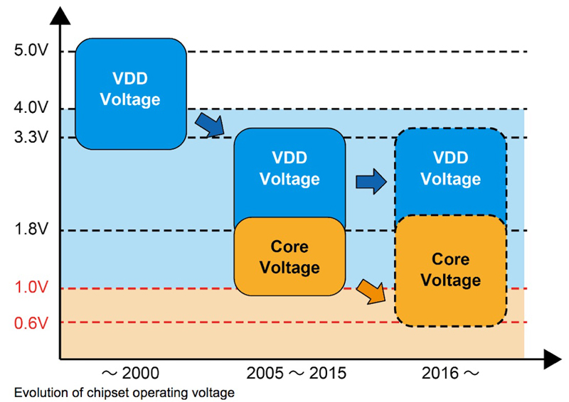
Click image to enlarge
Figure 1: Evolution of chipset operating voltages
Accuracy is an issue below 1V
Chipsets with an ultralow voltage operation are welcomed from the point of view of low device power consumption, however, there is an obstacle that must be overcome in order to incorporate these chipsets in a device. This obstacle is the “power supply” that converts the 3 to 4V battery voltage into a voltage for the chipset. This is because a higher accuracy is required of the power supply as the core voltage is reduced.
Of course, high accuracy is not the only characteristic that is required of power supplies that support ultralow voltage chipsets. “Small size” and “high efficiency” are universally demanded of power supplies used for wearable devices and communication modules, and these conditions must also be met. Furthermore, even if the power supply can supply a low voltage with high accuracy, a high self-consumption power and inferior conversion rate will negate the benefit of the low core voltage chipset. The appearance of small, high-efficiency power supplies that also supply a low voltage with high accuracy is eagerly awaited.
For example, the XC9272 high-efficiency step-down synchronous DC-DC converter can support an output from 0.6 to 0.95V. This power supply IC meets all of the required conditions, including a small size, high-efficiency, and the ability to supply a low voltage under 1V with high accuracy (see Figure 2).
Click image to enlarge
Figure 2: The XC9272 DC-DC converter achieves both high accuracy and ultralow consumption
Torex has been a leader of the industry in supplying power ICs for applications that have a strong need for small size and high efficiency such as wearable devices and communication modules. For example, the XC9265 Series, launched in 2015, features power ICs designed especially for wearable devices, which have long standby and long light load operation times, and this series achieves an ultralow self-quiescent current of 0.5μA, less than 1/30th the quiescent current of previous DC-DC converter products.
The series has a power conversion efficiency of over 80% even at a light load of 10μA. This efficiency is higher than that of LDO regulators, which are considered to have excellent efficiency at light loads.
There are two reasons that the XC9265 was able to achieve this low quiescent current and high efficiency: circuit design technology perfected by specialization in power supply ICs, and equipping the IC with PFM (frequency modulation) control mode, which has a comparatively good conversion efficiency at light loads, instead of the PWM (pulse width modulation) control mode that is common in DC-DC converters.
Support for low voltage output while maintaining a 0.5μA quiescent current
The new XC9272 for chipsets with a low core voltage under 1V was developed based the XC9265, which boasts a low quiescent current and high efficiency. While maintaining the two features of a 0.5μA quiescent current and good operation at light loads, the 1.0 to 4.0V output voltage (steps of 0.05V) on the XC9265 was adjusted to support 0.6 to 0.95V (steps of 0.05V).
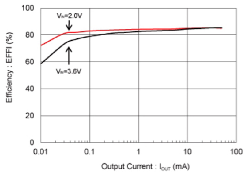
A design change was implemented on the XC9265 to enable support of 0.6V operation in part of the internal IC circuitry that previously operated based on a 1V or higher output voltage, making it possible to supply power to the latest low-voltage chipsets. Efficiency is over 80% even at a light load output of 0.7V/0.1mA and an input of 2.0V (see Figure 3). The accuracy that is a concern at low voltage outputs under 1V is ±20mV. This is sufficient for a 0.6 to 0.95V output DC-DC converter.
Click image to enlarge
Figure 3: Graph indicating efficiency of the XC9272
In practice, PFM mode generally has the drawback of a large ripple voltage. The effective result of a large ripple voltage is poor output voltage accuracy. Torex has minimized ripple voltage in two ways: analog circuit technology that makes it possible to use low ESR ceramic capacitors as recommended components, and optimization of product specifications for target applications such as wearable devices, mobile devices, and energy harvest devices. The 50mA output type of the XC9265 achieves a ripple voltage of 50mV, and now the XC9272 achieves a ripple voltage of 20mV at 50mA output, sufficient for practical use. The XC9272 is available in the same packages as the XC9265 (SOT-25 and 1.8 × 2.0 × 0.4mm USP-6EL), and in the same pin layout.
Increased battery life
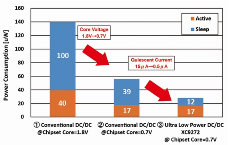
It appears that the XC9272, which combines the features of small size, high-efficiency, and the ability to supply a low voltage under 1V with high accuracy, will significantly extend the battery life of wearable and energy-harvesting devices. For example, in a configuration that combines a conventional 1.8V core voltage chipset with a conventional DC-DC converter (quiescent current about 15μA), the power consumption is 140μW 3.6V input, active mode at a 10mA load, 10 milliseconds, and a sleep mode of 10μA load 5 sec. In particular, the power consumption is 40μW in active mode and 100μW in sleep mode. This means that most power consumption occurred during the light load of sleep mode, in which the device spends the most time.
When the core voltage of the system chipset is reduced from 1.8V to 0.7V, power consumption can be significantly reduced to 17μW in active mode and 39μW in sleep mode, or a total of 56μW. However, the consumption in sleep mode is greater than in active mode, and this creates a bottleneck in extending battery life (see Figure 4).
Click image to enlarge
Figure 4: Comparison of power consumption by product and core voltage difference
When the ultralow 0.5μA quiescent current of the XC9272 is used with the core voltage of the chipset reduced to 0.7V, power consumption is reduced to 17μW in active mode and 12μW in sleep mode for a total of only 29μW. Compared to a conventional DC-DC converter, the power consumption is the same during operation, but is only 1/3 in sleep mode, and it is clear that the XC9272 maintains high efficiency even with light loads.
When we compare the battery drive times of the configurations, the result is even clearer. If the battery drive time of a system with a 1.8V core voltage chipset and a conventional DC-DC converter is “100”, reducing the core voltage to 0.7V extends the drive time to “250”. If the 0.7V core voltage chipset is combined with the XC9272, the drive time reaches “494”. This means that the XC9272 and a low voltage chipset can achieve 5 times the battery life of conventional devices at the same battery capacity (see Figure 5).

Click image to enlarge
Figure 5: Comparison of battery drive time by product and core voltage difference
A smartwatch that couldn’t even be driven for a day and a half can now operate for a week without being charged. With the appearance of low voltage chipsets and the XC9272, it looks like the battery life problem that has hindered the spread of wearable devices has been solved.