Hundreds of billions of dollars have been spent to make the silicon technology supply chain incredibly efficient. How can emerging, high performance GaN transistors compete against this huge installed base of silicon-based production? Simple, the production of GaN transistors leverages the installed silicon supply chain, which significantly lowers the cost of GaN transistors!
With the exception of the machines needed to grow the epitaxial GaN layers on top of silicon, all of the machinery needed to manufacture eGaN FETs is standard, trailing-edge equipment used to manufacture billions of silicon integrated circuits today. History shows that trailing-edge silicon wafer capacity is chronically abundant. The use of highly available and very mature capacity greatly reduces the amount of capital and the risk required to produce eGaN FETs in high volume.
The silicon suply chain
The starting point for today’s power MOSFET is the growth of a silicon crystal, followed by the growth of a thin layer of epitaxial silicon. These wafers are then processed through many tens, or even hundreds, of steps to produce a completed wafer with hundreds (or thousands) of individual transistors. Figure 2 is an image from the interior of a wafer fabrication facility showing the clean room and equipment common to semiconductor manufacturing. New wafer fabrication and test facilities like this cost several billions of dollars each to build and equip.
Testing is the next step where bad devices are identified to be removed at a later step. Following testing, the finished wafers are sent to a different facility to be saw-cut (singulated) into individual devices. Once singulated, the good devices are assembled into plastic packages, tested again to identify further rejects, packed and shipped to customers. On average, assembling MOSFETs into plastic packages account for about 50% of the total product cost.
The eGaN FET supply chain
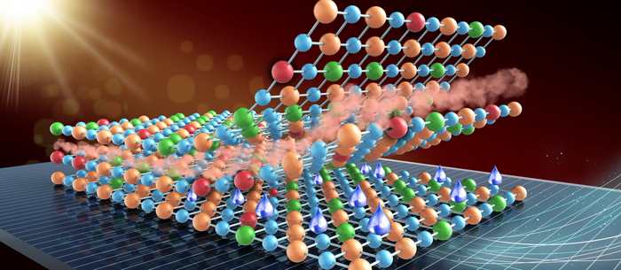
Like the power MOSFET, the current eGaN FET starting point is the growth of a silicon crystal. Instead of an epitaxial silicon layer, an epitaxial structure of aluminum nitride, aluminum gallium nitride, and gallium nitride is grown (This is called a hetero epitaxial structure). This growth is the only step that requires equipment specialized for GaN transistors. Both the epitaxial growth and the wafer fabrication today take place inside a commercial silicon foundry originally built in the late 1980’s to manufacture DRAMs.
This kind of trailing-edge capacity is widely available in the industry, and is perfectly adequate for producing state-of-the-art eGaN FETs because this technology is not as driven by smaller geometries. eGaN FETs also require far fewer process steps in the wafer fabrication process compared with advanced power MOSFETs.
As with MOSFETs, a testing step, whereby faulty die are identified for future segregation, follows wafer fabrication. Unlike the MOSFET, eGaN FETs, while still in wafer form, have a protective plastic coating applied and solderable bumps screen printed to form the electrical contacts to the outside world. This relatively low-cost sequence of steps for producing an eGaN FET replaces the costly and bulky plastic package needed for the silicon MOSFET.
With the exception of the machines needed to grow the epitaxial GaN layers on top of silicon, all of the machinery needed to manufacture eGaN FETs is standard, trailing-edge equipment used to manufacture billions of silicon integrated circuits today. History shows that trailing-edge silicon wafer capacity is chronically abundant. The use of highly available and very mature capacity greatly reduces the amount of capital and the risk required to produce eGaN FETs in high volume. There are about 10,000 transistors on this wafer. A comparable silicon MOSFET wafer would have only 2,000 to 3,000 devices. Singulation, packing and shipping are the final steps.
In the next couple of years, the bump, singulation, test, pack and ship steps will be integrated into the wafer fabrication facility. This consolidation will save cost and reduce the cycle time in the supply chain. It also improves flexibility and responsiveness to market fluctuations and reduces the amount of working capital needed to expand.
Capital investment and product Cost
With the exception of the machines needed to grow the epitaxial GaN layers on top of silicon, all of the machinery needed to manufacture eGaN FETs is standard, trailing-edge equipment used to manufacture billions of silicon integrated circuits today. History shows that trailing-edge silicon wafer capacity is chronically abundant. The use of highly available and very mature capacity greatly reduces the amount of capital and the risk required to produce eGaN FETs in high volume.
 PDF
PDF