Author:
Asem Elshimi, Silicon Labs
Date
06/01/2020
 PDF
PDF
Click image to enlarge
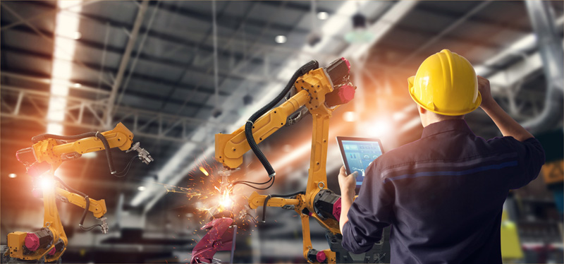
Figure 1. Isolators are essential to ensure the safety of both devices (machines and equipment) and human operators
Isolators are required to ensure our safety when operating equipment and to protect sensitive components within the equipment. They also maintain critical data (signal) integrity by providing immunity against external noise sources in safety-critical process control equipment. Countless devices must be isolated from the high-power domain.
For decades, engineers have used optical isolation technology that use light-emitting diodes (LEDs) – to isolate and protect devices and systems. However, legacy optocouplers are bulky and slow. Then in the late 1990s, the development of on-chip transformer-based isolators changed the game. In 2009, Silicon Labs introduced capacitive isolator ICs manufactured in mainstream CMOS. This innovation has transformed the design of multi-domain electrical systems. Digital isolation technology made the system designer’s job much simpler and easier and has enabled novel solutions that previously were impractical.
When electrical system designers need to bridge digital control signals or information between different power domains (usually, but not only, high-power and low-power), they can insert a digital isolator in the middle. The isolator IC handles all the isolation and communications with incredible efficiency and speed while ensuring safety. The idea is simple: a capacitive bridge or dielectric insulation, similar to how plastic insulation wrapped around copper electrical wires insulates the current. (Note one difference between insulation and isolation: While wire insulation does not allow any current across the insulation barrier, isolation allows data transfer while blocking current conduction.) Bringing this idea to fruition required an understanding of material science, IC design, packaging options, safety standards, emissions standards, and customer needs.
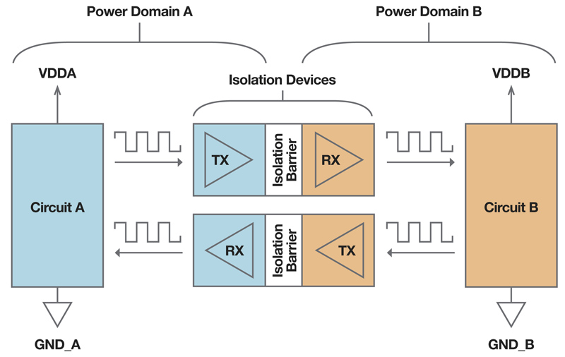
As shown in Figure 2, a capacitively coupled isolator functions like a capacitive bridge for the transmission and receipt of information across the isolation barrier. Capacitors are basically dielectric isolators. One of the first things we learn in engineering school is that dielectrics don’t conduct electric currents. Then at a more advanced level, when we see Maxwell’s equations for the first time, we learn that oscillations in dielectric dipoles under alternating currents (currents that are changing directions back and forth) lead to electric conduction of alternating currents. In short, dielectrics are selective of what currents they pass. That is the fundamental idea behind Silicon Labs’ capacitive isolators. We use silicon dioxide capacitive bridges to allow signal transmission (in AC current form) while isolating power domains.
Click image to enlarge
Figure 2. A simplified diagram of a capacitor-based silicon isolator
Isolators need to withstand a high working voltage. The voltage difference between different domains can go up to a few thousands of volts. Even the largest dielectric system in the world, our atmosphere, sometimes gets shorted by high voltage. Lightning is an arc conduction of charges between high potential clouds and the earth through the atmosphere. This phenomenon can also occur across capacitors, defining their breakdown voltages. Thanks to our deep understanding of material science and process technology, we design our capacitive isolators with a high breakdown voltage. That means a safer operation of isolator ICs over a longer time.
The main advantages of digital isolation over alternative isolator technologies such as optocouplers or transformer-based isolators are cost and size (which usually go hand in hand), communication speed, aging, and electromagnetic compatibility. While optocouplers come with the advantage of low electromagnetic radiation and immunity to external electromagnetic (EM) fields (as opposed to transformer-based solutions, which use magnetic coupling to transfer signals), they are bulky.
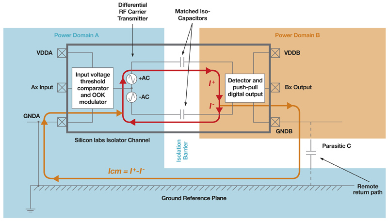
Si86xx digital isolators from Silicon Labs are high-performance, wide-channel-count uni- and bidirectional isolation ICs supporting up to 5 kV isolation ratings. It only takes about 13 nanoseconds for a signal to cross the Si86xx IC’s capacitive barrier. While a capacitor on its own can radiate electromagnetic power and corrupt operation of nearby devices and instruments, capacitive isolators are designed to minimize radiated emissions. One of many tricks that our capacitive isolators have is differential signaling, which uses two capacitors across the bridge that always carry opposite currents. If one radiates positive EM energy, the other capacitor absorbs this energy. This means the net radiated EM energy is zero, greatly minimizing the isolator IC’s EM radiation. Low EM makes capacitive couplers ideal for electromagnetic-sensitive environments such as power supplies or biomedical solutions. Biomed environments can be particularly challenging when it comes to EMI management, especially since some medical equipment, such as MRI systems or wireless medical telemetry systems, uses RF energy for diagnosis or treatment.
Isolation and Sustainability
Nowadays there is an enormous focus on sustainability and green energy technology. Reducing carbon emissions and leveraging renewable energy resources are now a top priority for governments and people everywhere. Solar energy panels and EVs are integral to a sustainable energy future. The solar panel industry is experiencing exponential growth. In 2019, 13.3 gigawatts (GW) of solar PV capacity was installed in the US to reach 77.7 GW of total installed capacity, enough to power 14.5 million American homes. Solar energy accounted for 40 percent of all new electric generating capacity added to the grid in 2019 – more than any other energy source and the highest share in the industry's history. [Source: https://www.seia.org/us-solar-market-insight]
To sustain this exponential growth and help shape a cleaner future, the green energy industry needs every bit of innovation. For example, solar technologies rely on electronics and digital processing to optimize system performance. Every improvement in inverter technology reduces the cost of solar panels and improves the total efficiency of each panel. These advancements will encourage the wider adoption of solar energy.
The inverter is basically a power converter. It takes DC power generated from the panel and delivers AC power to the utility grid. The photovoltaic inverter acts as a bridge between two power domains and uses isolators to achieve this task. In a solar power conversion system, different types of isolators are adopted to serve various functions. Isolated gate drivers are used to drive insulated gate transistors such as Silicon Labs’ Si822x and Si823x devices. Isolated analog-to-digital converters (ADCs) and isolated amplifiers are used to sense and convert analog front-end signals such as voltages and currents to enable closed-loop controls.
Solar PV systems will undoubtedly continue to evolve to meet market demands for higher capacity, lower cost, and higher reliability. As this happens, PV inverters will expand in functionality, and designers will demand more integrated, application-specific, component-level devices to further leverage and drive innovation in CMOS isolation. As these events unfold, PV power systems will become more widespread and ultimately represent a viable segment of mainstream utility grids that will significantly reduce our dependence on fossil fuels.
Click image to enlarge
Figure 3. One of the many tricks that capacitive isolators use is differential signaling
As this happens, the utility grid will need to adapt. Consumers with solar panels are now producing energy, and an advanced smart grid enables consumers to transfer power to the utility grid. Inevitably, storing instantaneous generated renewable energy must be addressed. One of the most attractive solutions is storing excess energy in large-scale battery arrays. While such a vision is still evolving, it is obvious that separate power domains are coming closer and must be connected while still isolated. This development will help grow a bigger market opportunity for isolator ICs, requiring further technology innovation and improvement.
The electric vehicle (EV) market has witnessed a rapid evolution in recent years with the ongoing developments in the automotive sector. The global EV market is projected to reach 26,951,318 units by 2030 from an estimated 3,269,671 units in 2019, at a CAGR of 21.1 percent during the forecast period.
[Source: https://www.marketsandmarkets.com/Market-Reports/electric-vehicle-market-209371461.html] (Note: This EV market projection preceded the COVID-19 outbreak, and EV growth may slow down until the pandemic is under control.)
The EV market is relatively new compared to other green energy markets. While more established markets were drawn to optocouplers from a familiarity standpoint, EV battery management system designers saw the advantage of capacitive coupling from the beginning. The high voltages and noisy environments in EV drive systems require robust, high-performance galvanic isolation to ensure safe and reliable operation. Ever-increasing power densities from raising the wattages and shrinking the sizes of EV subsystems create demanding thermal and electrical noise conditions. CMOS-based isolation offers significant advantages over legacy optocoupler solutions, which make them an ideal choice in demanding EV systems and other sustainable energy applications including solar and wind power inverters.