Date
06/16/2016
 PDF
PDF
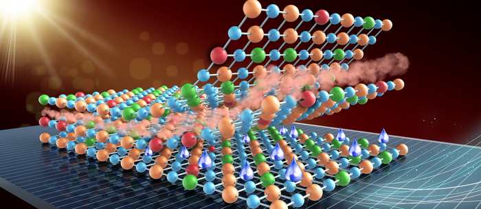
At the 2016 Symposia on VLSI Technology & Circuits, nano-electronics research center imec presented junction-less gate-all-around (GAA) nanowire (NW) FETs built in lateral and vertical configurations. With their simplified processing, improved reliability, reduced low frequency noise and lower IOFF values, they are an attractive option for advanced logic, low power circuits and analog/RF applications. Moreover, they enable a simpler path for considerable SRAM scaling via the stacking of vertical devices.
GAA-NWFETs -with the gate fully wrapped around the device body for optimum electrostatics control- are considered one of the most promising candidates for enabling (sub-)5nm CMOS scaling. Moreover, junction-less devices offer great process simplicity as they do not require junctions.
Previously, at the 2015 VLSI and IEDM conferences, imec demonstrated the superior reliability behavior of these devices and their potential for low power circuits. At today’s VLSI symposium, imec thoroughly evaluated key control knobs for junction-less devices operation, namely controlling the NW doping vs. NW size to achieve optimum performance. The feasibility of these devices for analog/RF applications was also studied, concluding them to be a viable option with reported similar speeds and voltage gains as compared to inversion-mode NWFETs.
Imec also addressed the variability of junction-less GAA-NWFETs, showing that whereas the VT mismatch increased with increasing nanowire doping for NMOS devices, less impact was observed for PMOS devices and at smaller nanowire dimensions.
Additionally, the junction-less concept was demonstrated in vertical devices integrated on the same 300mm Si platform, also used for lateral devices. Low IOFF and IG values and good electrostatics were achieved over a wide range of vertical nanowire arrays.
Lastly, taking advantage of the junction-less devices process simplicity, Imec further explored their potential by proposing a novel SRAM cell design with two vertically stacked junction-less vertical NWFETs with the same channel doping, thus enabling reduction of the SRAM area per bit by 39%.
“Imec’s work has contributed to an increased and more in-depth understanding of junction-less GAA-NWFETs,” stated Dan Mocuta, Director Logic Device and Integration at imec. “Our thorough evaluation highlighted the excellent performance of junction-less lateral and vertical nanowire devices for beyond 5nm logic devices. Moreover, junction-less devices appeared as a viable option for analog/RF applications, whereas stacked junction-less vertical nanowire FETs could significantly reduce SRAM area.”
Imec’s research into advanced logic scaling is performed in cooperation with imec’s key partners in its core CMOS programs including GlobalFoundries, Intel, Micron, SK Hynix, Samsung, TSMC, Huawei, Qualcomm and Sony.