Click image to enlarge
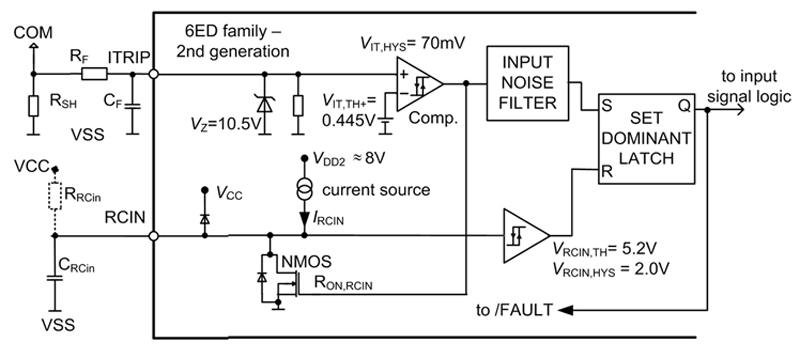
Figure 1: Internal structure of the ITRIP and RCIN sections
The megatrends in consumer drive systems are unbroken: The numbers of units are growing and so are the number of comfort features and quality requirements for the drive. With Infineon's SOI technology the integrated circuits on the top side of the IC are separated from the deep substrate by a buried silicon oxide layer. The buried silicon oxide provides an insulation barrier between the active layer and silicon substrate and hence reduces the parasitic capacitance tremendously. Moreover, this insulation barrier disables any kind of leakage or latch-up currents between adjacent devices. This results in an extremely high robustness against any kind of negatively biased nodes which are connected to the IC. As an example, the motor phase node is allowed to dive below the VSS potential down to -50 V for duration of 500 ns, which is the largest rectangular negative transient SOA of monolithic gate driver IC worldwide. The available devices are high-voltage and low-voltage MOS transistors, different diodes and passive elements like capacitors and resistors of various values.
Special feature set The 6ED family - 2nd generation contains various comparators which are helpful in the application in order to avoid external circuits of external comparators and their biasing circuits. This section describes the individual functions and features. Safety relevant shut down options The 6ED family - 2nd generation offers a couple of independent options for a shutdown of the inverter. First of all, the enable comparator can be used. The signal applied to pin EN controls directly the output sections. All outputs are set to LOW, if the signal is lower than VEN- = 1.3V typically and operation is enabled with signal levels higher than typical VEN+ = 2.1 V. The internal structure of the IC contains a Schmitt-Trigger. The typical propagation delay time from EN to the output sections is here tEN = 780 ns. The IC is steadily enabled, when the EN pin is pulled up to VDD (i.e. +5V / +3.3V). It is not recommended at all to pull this pin up to VCC, because this may lead to excessive power dissipation in the input structure of this pin and could destroy the IC. The second and most striking feature is the comparator at pin ITRIP. The comparator's threshold is designed to be directly connected to a low inductance shunt resistor RSH by means of an RC filter (RF, CF) according to Fig.1. The output of the comparator passes a noise filter, which inhibits an over current shutdown caused by parasitic voltage spikes. The typical filter time of the noise filter is tITRIPMIN = 210 ns. A set-dominant latch stores the over current event until it is reset by the signal provided from the RCIN circuit. The ITRIP-comparator activates also the discharging NMOS-FET at pin RCIN. The RDS(on) of the FET is typically 40�?, so that there is a characteristic discharge curve in respect of the external capacitor CRCin. The time constant is defined by the external capacitor CRCin and the RDS(on) of the FET. The discharge phase ends, when the comparator output at pin ITRIP is low again. This corresponds to a voltage level at the comparator of VIT,TH+ - VIT,HYS = 445 mV - 70 mV = 375 mV, where VIT,HYS = 70 mV is the hysteresis of the ITRIP-comparator. The failure status is latched for a user programmable time, which is the charging time constant of the external capacitance CRCin and the internal current source. The source provides the current IRCin. Thanks to the current source an additional external charging resistor is not required. The /FAULT signal is activated while the failure status is latched.
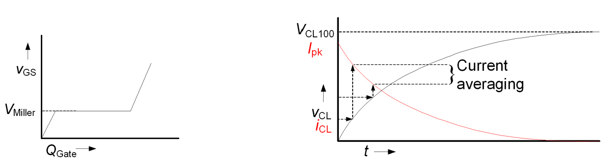
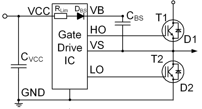
Integrated bootstrap diodes The integration of bootstrap diodes into 6EDL04I06NT, 6EDL04I06PT, 6EDL04N06PT and 6EDL04N06PR is the most striking achievement of the new generation of 6 channel gate driver IC. Bootstrapping is the common way to supply floating high side sections and was done by means of 600 V ultra fast switching diodes and a current limiting resistor in series. The ultra fast switching diodes are the simplest way to have a charging current to CBS, when the node VS is virtually GND, i.e. when the low side IGBT T2 is turned on according to Fig.2. Using the 6ED family- 2nd generation saves therefore up to three resistors and three ultra fast 600V diodes. Large forward resistance values can lead to large voltage variations on the bootstrap capacitor as a result of sinusoidal pulse width modulations (PWM). It can be shown analytically, that this can even lead to temporary under voltage lockout situations, which must be overcome by large bootstrap capacitor values. The 6ED family - 2nd generation now offers much smaller forward resistance, which helps to keep the bootstrap capacitor small and cheap. Furthermore, the 6ED family specifies also a maximum value of 60 ?, where none of the market competitors do. Furthermore, bipolar structures such as diodes are more robust against temperature increase in terms of forward characteristic. That means that the use of a real bootstrap diode widens the area of operation, whereas the use of integrated FET structures reduces the area of operation even more. Negative Transients at High Side Reference (pin VSx) The 6ED family - 2nd generation is very robust against negative transient voltages thanks to the inherent oxide insulation of the SOI-technology. Such transients may occur due to stray inductances in the physical setup. Parasitic inductances can induce voltages vind(t) , which have an amplitude ? of the duration T so that the potential at pins VS1, VS2 or VS3 becomes negative in respect to pin VSS. It is a well known failure mechanism of other driver IC technologies that these negative voltages force current through the substrate material. The substrate currents can lead to a latch of the high side gate driver, which is then insensitive to any control signal for several milliseconds. The result is, that the IGBT are operated in repetitive short circuit, which leads to excessive power dissipation and finally also to system breakdown. Therefore, the minimum voltage at the pins VSx is specified to -50 V for a period of time of 500 ns. This duration is long enough to cover the usual requirement for this stress in drives applications. Usual switching transitions are finished inside this window. However, it must be the target of any design to avoid such negative voltages at all. The negative voltage can also increase the pulse current through the external or internal bootstrap diode and may lead to damage. The design target is therefore to avoid such negative transient voltage at all or to keep at least the absolute maximum ratings. Output current characteristics The output current characteristic shows typical sink currents of 380 mA and source currents of 170�mA. The test condition gives a helpful condition for design engineers. The switching transition of power transistors takes place, when the gate voltage reaches the miller voltage according to Fig.3. The miller voltage is approximately between 5V - 7V. It is important to have a sufficient gate current capability in this area in order to avoid being too long in the linear region of power transistors and to reduce switching losses. It is therefore especially the current capability in the miller region, which is important for the application. The test condition of the 6ED family - 2nd generation is specified to the average output current in a window between 20% and 40% of the gate voltage amplitude according. One can see that this covers well the area of the miller voltage and the application can be nicely fine tuned. It is easy to understand, that other output current specification such as a short circuit condition, is not appropriate here to fine tune the application. However, characterization measurements show, that the 6ED family - 2nd generation also provides competitive values for the short circuit test condition. Conclusion The 6ED family - 2nd generation is an innovative and intelligent driver IC. Its various options for shutting down the inverter offer a lot of opportunities to fine tune the application. The integrated bootstrap diodes can save external components on the system side. The gate drive outputs are powerful enough for all consumer drive applications and home appliances. www.infineon.com
 PDF
PDF