Author:
David New, Product Marketing Manager for computing applications Power Integrations, Inc., San Jose, California. US
Date
01/15/2011
 PDF
PDF
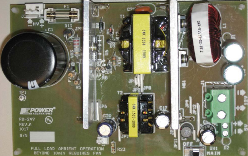
Click image to enlarge
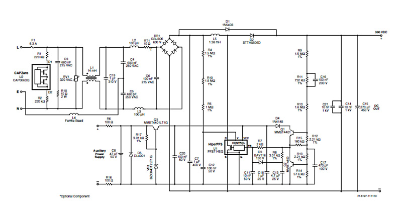
Figure 1: 347W universal input PFC
Power supplies of up to1kW output power account for the majority of power supplies used in high-volume electronics applications. One obvious application that we use every day is the personal computer, but other examples include printers, TVs, video game consoles, appliances, and industrial equipment. Designing power supplies for these products is becoming more challenging due to several, sometimes conflicting, factors. Power supplies are required to fit into ever more compact form-factors, making design, assembly, reliability, and thermal management more difficult. Higher efficiencies are also desired to meet current and emerging energy-efficiency regulations and to simplify thermal management. Finally, these power supplies often need to meet standards governing electromagnetic interference (EMI), total harmonic distortion (THD), and power factor (PF). One solution - perhaps the most cost effective - is the use of advanced semiconductor power management products that employ sophisticated control techniques and highly efficient, high-frequency power MOSFETs. By taking a system approach to power supply design, Power Integrations Inc. (PI) has developed a power supply solution with essentially only two ICs, an active power factor correction chip and a DC-DC converter. Power Factor Correction Poor PF and high distortion of current drawn by electronic equipment is a major concern for power distribution networks. To enforce a limit on the amount of harmonic distortion and PF degradation caused by electrical and electronic equipment, standards like IEC/EN61000 and ENERGY STAR® stipulate limits of the harmonic distortion and PF requirements for many different classes of equipment. A simple way to improve the PF and reduce THD is to use a passive PFC circuit. However, passive PFC circuits tend to be less efficient than their similarly-sized active PFC counterparts and they can be large and expensive at higher power levels. Active PFC circuits can provide higher PF and lower THD for a given cost and form factor. Active boost PFC circuits are able to boost their output voltage to a higher voltage (e.g., 380V) over a wide range of line input voltages. This regulated high-voltage output provides a stable input to a secondary converter. Often these secondary converters are isolated DC-DC converters that benefit from the high input voltage because the primary side currents are lower for a given power level, allowing lower I2R losses and reduced cost. Single-Chip, High-Power PFC Power Integrations' HiperPFS™ device family members incorporate a variable frequency continuous conduction mode (VF-CCM) boost PFC controller, gate driver, and high-voltage power MOSFET in a single, low-profile eSIP™ power package. HiperPFS devices eliminate the active PFC converter's need for external current sense resistors and leverage an innovative control technique that adjusts the switching frequency over output load, input line voltage, and even input line cycle. By this means HiperPFS enables >96% efficiency to be achieved over 10% - 30% load. Additionally, the control technique significantly minimizes the EMI filtering requirements due to its wide-bandwidth spread spectrum effect. Systems using HiperPFS typically reduce the total X and Y capacitance requirements of the converter and the inductance of both the boost choke and EMI noise suppression chokes. HiperPFS' novel control method produces a continuous mode power switch current waveform that varies both in frequency (typically 24 to 95kHz) and peak current value across a line half cycle. This produces an input current that is proportional to the input voltage throughout the waveform cycle, hence a PF of close to unity. Application in Practice Figure 1 shows a complete application schematic of HiperPFS. This design is rated for a continuous output power of 347W and provides a regulated output voltage of 380VDC nominal. The circuit forms a general-purpose power factor corrected input stage for a switch-mode power supply meeting energy-efficiency standards such as the European Code of Conduct, 80 PLUS®, and ENERGY STAR. The design is scalable, with minimal changes required for outputs of up to 1kW.
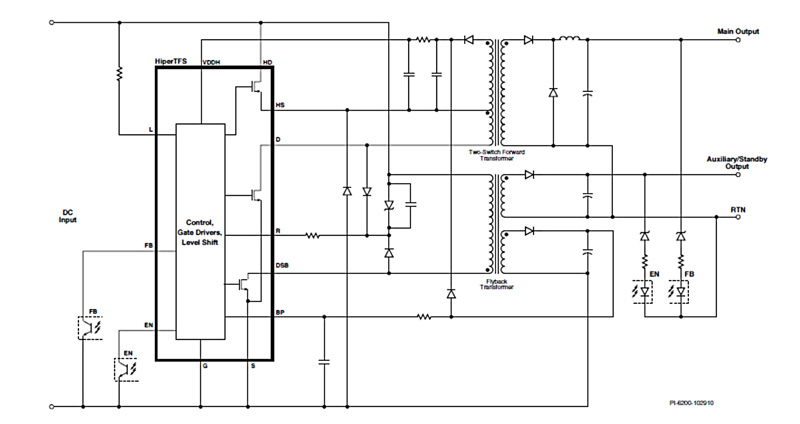
Note that the circuit is considerably simpler, using up to 40 fewer discrete components, than required for less integrated solutions with separate controller ICs and discrete MOSFET switches. The CAPZero™ (U2) device at the AC input is another novel device from PI that contributes to increasing light-load efficiency. Resistors R1 and R2 are required to discharge the EMI filter capacitors whenever the circuit is disconnected from the AC supply. CAPZero eliminates static losses in R1 and R2 by only connecting the resistors across the input when the AC voltage is removed. The PFC's boost converter stage consists of inductor L5, diode rectifier D2, and the HiperPFS IC (U1). Designing for High-Power Applications There are many topologies to choose from when designing a high-power power converter. Single-switch forward, two-switch forward, and series resonant converters are just a few. For a good balance between cost and efficiency, two-switch forward converters are chosen for many cost-sensitive, high-power designs. Generally, an auxiliary converter is also required to provide standby power and startup management. HiperTFS™ ICs from PI incorporate both a high-power two-switch forward converter and a mid-power flyback (standby) converter into a single eSIP™ power package. HiperTFS includes the controllers, high- and low-side drivers, and all three of the high-voltage power MOSFETs. It is ideal for high-power applications that require both a main power converter of 150W to 415W and standby converter up to 20W. The schematic in Figure 2 shows how HiperTFS provides the power management for both main and standby converters.
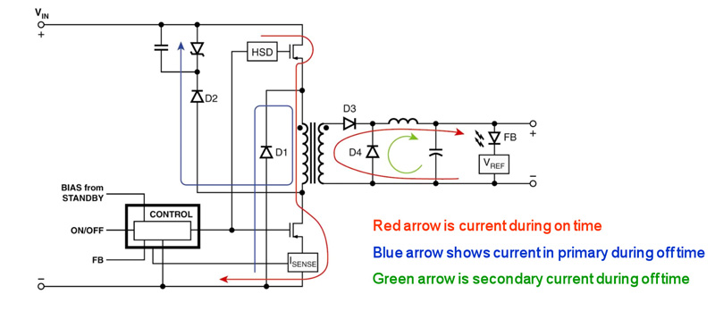
The two-switch forward controller incorporated into HiperTFS devices improves on the classic topology by allowing operation considerably above 60% duty cycle. The two-switch forward topology involves a low-side and high-side power MOSFET, both of which are switched at the same time. When the MOSFETs are on, energy is coupled from primary to secondary via the transformer (as shown in Figure 3). The main transformer is a coupling element only (no core gap). During the conduction phase, the output inductor stores energy and current is supplied directly to the load. When the MOSFETs switch off, stored energy in the inductor is released and current continues to flow to the load, free-wheeling through diode D4. The input voltage rail plus DC-offset clamp resets the transformer, providing a highly efficient reset and recovery of leakage inductance energy. The DC-offset clamp capacitor, in series with D2, creates the asymmetric characteristic, and the maximum value is limited by the parallel Zener diode.
HiperTFS' asymmetrical operation reduces RMS current conduction losses (>30% typical reduction in RDS(ON) losses), minimizes the size and cost of the bulk capacitor, and minimizes output diode voltage ratings. The IC's cycle-by-cycle transformer flux reset control prevents core saturation under all conditions, and the charge-recovery switching of the high-side MOSFET reduces switching losses. This combination of innovations yields an extremely efficient power supply with fewer components and lower assembly costs. Figure 4 is an example of a design using HiperTFS providing a 300W, +12V output forward-derived main converter and a 15W, +5V standby output from the flyback converter. The very high integration of HiperTFS results in a very low external parts count, with a reduction of 30 or more components when compared with conventional designs. The design is scalable above 400W with minimal changes required. Conclusion HiperPFS and HiperTFS highlight the advances we are seeing in today's power management solutions for designs in the sub-1kW power supply sector. The two design examples described demonstrate the potential for significant cost and size reduction, while providing high efficiency, power factor close to unity, and easily achieving THD and EMI regulations. www.powerint.com