Author:
Zhijun (George) Qian, Senior Engineer, Analog Devices, William Xiong, Applications Engineer, Analog Devices
Date
03/02/2020
 PDF
PDF
Click image to enlarge
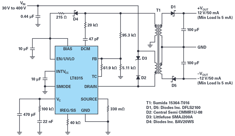
Figure 1. A complete ±12 V/50 mA isolated flyback converter for a wide input range, 30 V to 400 V.
Electric vehicles, large-scale battery storage stacks, home automation, industrial, and telecom power all require converting high voltages to ±12 V, where dual polarity rails are required for powering amplifiers, sensors, data converters, and industrial process controllers. One challenge in all of these systems is creating a compact, efficient dual polarity regulator that can operate over a temperature range of –40°C to +125°C — especially important in automotive and other high-ambient temperature applications.
Linear regulators are well understood and typically top the list of candidates for bipolar supplies, but are not suitable in the high input voltage, low output voltage applications previously mentioned, mainly due to heat dissipation in the linear regulator at high step-down ratios. Furthermore, a dual polarity solution requires at least two integrated circuits (ICs): one positive output linear regulator and a negative converter. To achieve better efficiency and regulation, as well as reducing footprint and cost, an alternative approach is to use a single switching regulator that produces both outputs from a relatively high input.
This article presents two elegant circuits that generate ±12 V outputs from a wide 30 V to 400 V input voltage range, both using a single high voltage converter. One circuit is an isolated flyback topology while the other is based on a nonisolated buck topology. To illustrate these circuits, we will use the LT8315, a high-voltage monolithic converter with integrated 630 V/300 mA MOSFET, control circuitry, and high voltage start-up circuit all inside a thermally enhanced 20-lead TSSOP package.
Isolated Dual Polarity Flyback Regulator with No Optocoupler
Flyback converters are widely used in multi-output applications to provide galvanic isolation, improve safety, and enhance noise immunity. Outputscan be positive or negative, depending on which side of the output is grounded. Traditionally, the output voltage regulation is achieved using optocouplers to transfer information from the secondary-side reference circuitry to the primary side. The problem is that optocouplers add significant complexity and degrade reliability due to propagation delay, aging, and gain variation, etc. Typically, the one output connected to the feedback pin of the IC dominates the regulation loop, while other outputs are loosely controlled through the transformer windings, resulting in poor regulation of those outputs.
For these circuits, the LT8315 requires no optocoupler and samples the reflected, isolated output voltage from a tertiary winding on the power transformer. Also, the output voltage is sensed when the secondary current is almost zero to achieve excellent load regulation. In a dual output design, this sensing scheme allows each output to be closely regulated — both outputs can dominate the regulation. As a result, a typical ±5% load regulation is easily achieved.
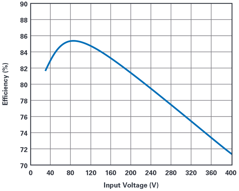
The isolated flyback converter circuit shown in Figure 1 operates under quasi-resonant boundary conduction mode and has a wide input range of 30 V to 400 V. It outputs ±12 V and maintains tight regulation with load currents from 5 mA to 50 mA. The primary MOSFET has a minimum turn-on loss because the MOSFET turns on when the switch node rings to its valley. There is no diode reverse recovery loss on the secondary side. A 3 kV reinforced insulation transformer is the only component across the isolation barrier, enhancing system reliability and meeting stringent high voltage power isolation requirements. Figure 2 shows the full load efficiency curve under different input voltages. This flyback converter achieves 85.3% peak efficiency when the input is 70 V and both load currents are 50mA.
Click image to enlarge
Figure 2. This graph shows full load efficiency vs. input voltage for the flyback converter in Figure 1.
Nonisolated Dual Polarity Buck Regulator with Two Inductors
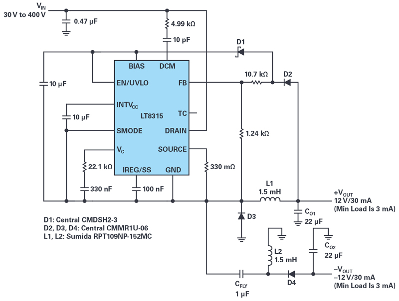
This high-voltage input approach can be applied in nonisolated situations as well by using off-the-shelf inductors. A buck regulator with dual inductors, requiring only a few components, is shown in Figure 3. This converter accepts an extremely wide-ranging input—30 V to 400 V—and produces ±12 V/30 mA outputs. This circuit can achieve efficiency as high as 87% at full load for both outputs with a 30 V input.
Click image to enlarge
Figure 3. Schematic of a nonisolated dual inductor buck converter using a single LT8315 IC: 30 V to 400 V input to ±12 V outputs at 30 mA each.
In this topology, LT8315’s GND pad is intentionally ungrounded and connected as the common switch node for driving both outputs. For PCB layout, GND pad size should be constrained within the exposed pad area to reduce electromagnetic interference to other components because the GND trace is a relatively noisy switch node in this topology. Diode D2 and two 1% resistors at the FB pin form the feedback path regulating the positive output voltage. D2 is necessary to prevent the FB pin discharging whenever the MOSFET conducts. The resistive voltage divider does not need to take into account the forward voltage drop of D2 because the forward voltage of D2 and D3 are equal and cancel; therefore, the feedback network tracks and closely regulates the positive output voltage.
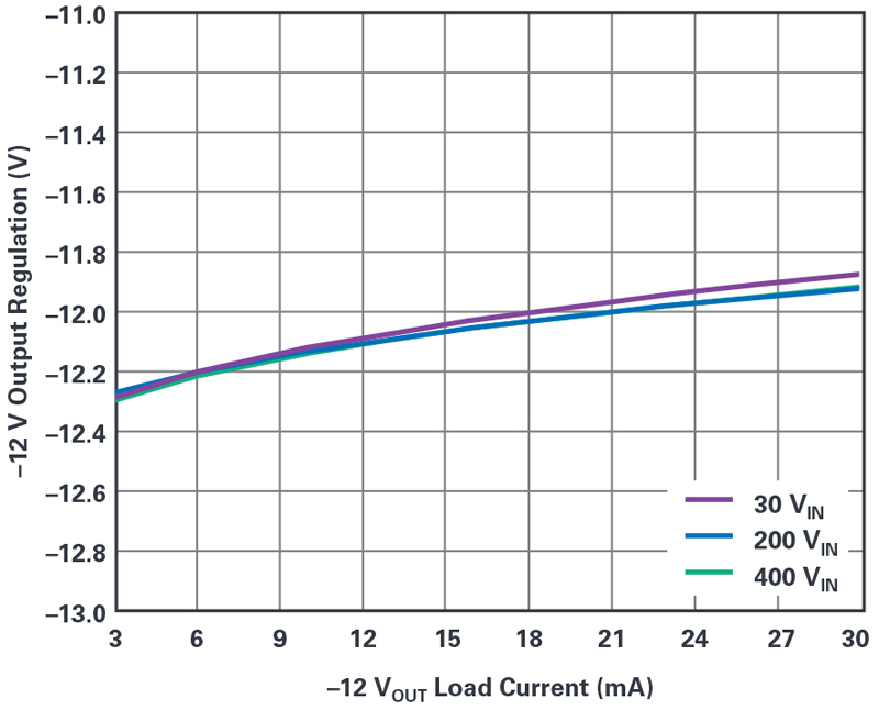
The negative rail comprises a low voltage coupling capacitor CFLY, a second inductor L2, a catch diode D4, and the negative output capacitor CO2. According to the inductor volt-second balance for the circuit loop of CO1-L1-CFLY-L2, the average voltage across L1 and L2 is zero, so the coupling capacitor CFLY’s voltage is equal to the positive output voltage. CFLY charges up L2 during the on-time of the MOSFET, while D4 provides a path for the L2 discharge during the MOSFET off time. The negative output voltage is indirectly regulated based on the voltage of CFLY remaining constant and equal to the positive output voltage. As shown in the regulation curve of Figure 4, the negative supply maintains ±5% regulation for a load range of 3 mA to 30mA at various input voltages, when the positive load is at a full 30 mA.
Click image to enlarge
Figure 4. Negative 12 V load regulation curves at various input voltages for the dual inductor buck converter in Figure 3.
This article presents two dual polarity converter solutions for a wide 30 V to 400 V input range: one isolated, the other nonisolated. A single switching regulator is used in both, utilizing a high-voltage integrated MOSFET, no optocoupler feedback loop, and internal high voltage startup circuit. Other regulator capabilities include low ripple Burst Mode operation, soft start, programmable current limit, undervoltage lockout, temperature compensation, and low quiescent current. By taking advantage of integration of the integration available in today’s regulators, developers can simplify the design of high-voltage input and dual polarity output circuits for a wide variety of applications.