Author:
Bob Callanan, Applications Manager and Julius Rice, Applications Engineer, Cree
Date
11/19/2012
 PDF
PDF
Click image to enlarge
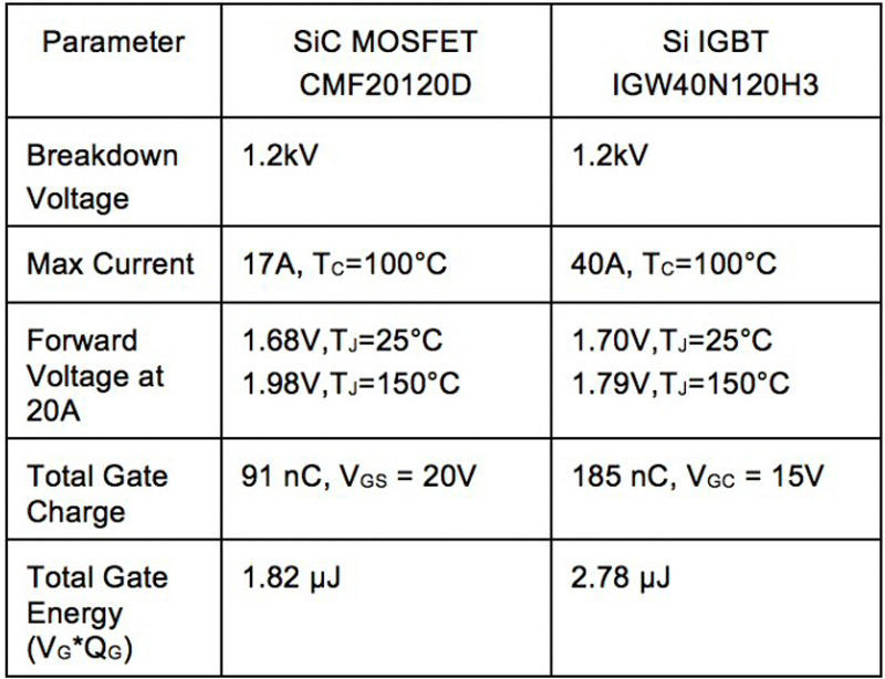
Table 1: SiC MOSFET and Si IGBT comparative specifications
To demonstrate the advantages of silicon-carbide MOSFETs versus silicon IGBTs (insulated-gate bipolar transistors) when used in high-power, high-frequency circuits, it is necessary to employ a test platform that will showcase each device's power handling characteristics—especially switching losses—under hard-switched conditions. A SEPIC (single-ended primary-inductance converter) test platform provides a means to emulate a set of established circuit parameters, such as switching frequency, voltage, current, and temperature. It also provides a means to calculate the differences in device losses between the two different power-switching technologies. The results of this test platform demonstrate that SiC MOSFETs have up to three-times higher operating frequency with the same efficiency, only 10% of the turn-off losses, and significantly lower relative switching losses as comparably rated Si IGBTs at 30 kHz. Comparison of switching performance This demonstration compares a Cree CMF20120D1 1.2-kV, 20-A silicon-carbide MOSFET (reference 1) and an Infineon IGW40N120H32 1.2-kV, 40-A silicon IGBT, which is a trench-stop field power device (reference 2). The IGBT exhibits a forward voltage at 20 A that closely matches the SiC MOSFET. Both devices were packaged in TO-247 plastic packages and mounted on identical connectorized daughter-boards with equivalent heat sinks, which enabled the two components to be swapped out quickly and efficiently for the test procedure. Table 1 compares the specifications for the two devices.
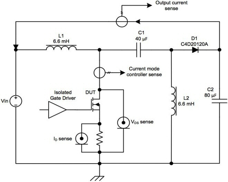
Selection of the SEPIC platform for circuit comparison Developing a single test platform to compare the switching performance of these two device technologies required a transformerless DC-DC converter design that re-circulated the load current back into the input link. This avoids the hardware issues that arise with transformers operating at high frequencies, such as proximity and skin effects in the windings and excessively high switching losses. The SEPIC platform delivers the flexibility to buck or boost without inverting the output voltage, making it a good choice to compare the relative switching performance and device losses between SiC MOSFETs and Si IGBTs. With the SEPIC platform, it is possible to demonstrate the switching performance of the power devices without re-designing and retrofitting each potential application (motor drives, power-factor-correction circuits, grid-interfaced solar and wind inverters, and uninterruptible power supplies) with SiC-based devices and then comparing the overall system performance for each application. The SEPIC demonstration platform features a simple buck-boost design with the ability to re-circulate the converter's output current back to the input side, while maintaining the devices under test (the power switches) at a duty cycle of approximately 50% (figure 1). This results in the voltage across the switch being twice the output current. Therefore, the input DC supply is only required to deliver half the desired switch voltage. Also, by referencing the switches to ground, accurate measurements of their voltage and current are easy to perform. The SEPIC schematic consists of the DUTs (device under test), which are the swappable power switches being tested; a blocking capacitor, C1; two inductors, L1 and L2; and a diode, D1. As shown by the directional arrows, the output current feeds back into the input source, VIN. A peak-mode current controller feeds from the current transformer to the DUT's drain connection. Meanwhile, the input for this controller is supplied from an amplifier that regulates the re-circulated output current. A Hall-effect sensor monitors this output.
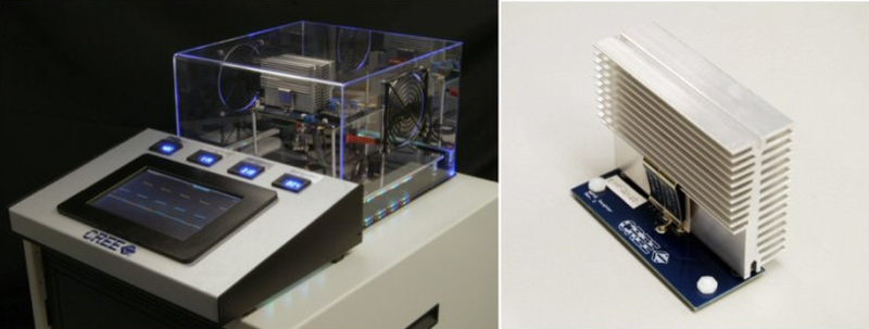
Other diagnostic elements of the SEPIC platform include a high-frequency current-monitoring resistor that senses the DUT current, and a voltage probe featuring a Kelvin connection to measure the DUT voltage. Isolating the gate driver eliminates the potential to form a ground loop around the resistor. The high-voltage components and logic power supplies used in the SEPIC demonstration platform and the inductors share an enclosure, with the control panel and converter hardware on top of the assembly protected by an acrylic safety barrier (figure 2). Test results display on a monitor that shows voltage and current waveforms for the devices under test and meters display total delivered power, total delivered current, total system losses, and input power.
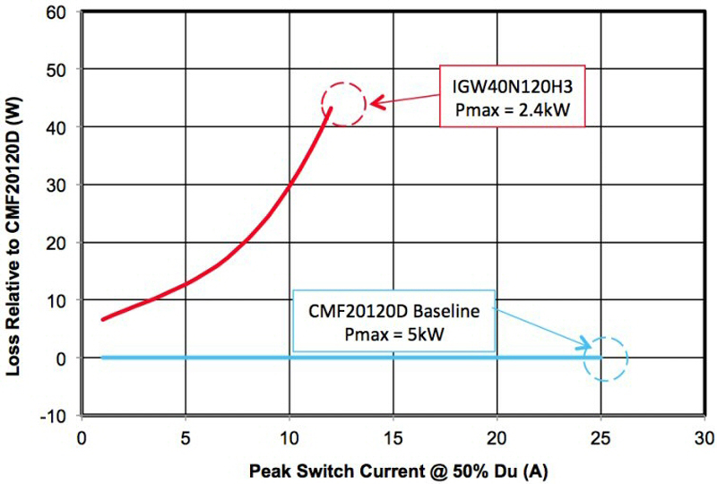
Performance comparison at 30 kHz Using the input power versus peak switch current for the SiC MOSFET as a baseline, the comparative switching losses are shown by subtracting this data from the input power versus peak switch current of the Si IGBT. The devices were tested under identical conditions of voltage, current, and frequency using the same circuit. The difference in input power between the two devices, therefore, is a direct measurement of their respective switching losses. The Si IGBT's input power loss relative to the SiC MOSFET was plotted against the peak switch current (figure 3). For this portion of the testing at 30 kHz switching frequency, the input voltage to the SEPIC circuit was 400 V, resulting in a switch voltage of 800 V. The test terminated when it exceeded the DUT's thermal limits. The SiC MOSFET achieved the highest switch current—25 A—with 5 kW of delivered power; while the Si IGBT reached a maximum switch current of 12 A with 2.4 kW of delivered power; with the IGBT's switching losses being the limiting factor
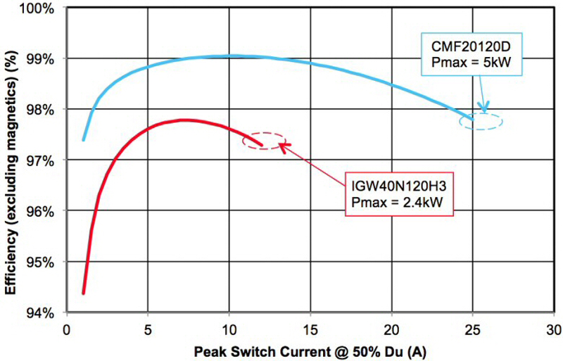
It is also possible to show the devices' relative efficiency as opposed to relative power losses. The switching devices themselves have low-loss characteristics, although the inductors (as part of the SEPIC circuit) have much larger losses (I2R); however, these losses are predictable. Therefore, by subtracting out these inductor losses from the total system losses, it is possible to see the relative switching efficiency of the devices under test. Plotting the switch efficiency versus peak switch current demonstrates that the SiC MOSFET is the higher efficiency device, delivering 5 kW of power; while the Si IGBT delivers just 2.4 kW, with an efficiency about 1.2% lower than the SiC device (figure 4).
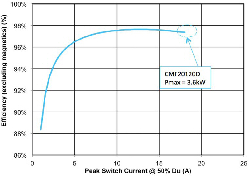
Switching performance at 100 kHz While testing at a frequency of 100 kHz, the silicon IGBT exhibited switching losses that are so high that hard-switched operation was impractical. Conversely, the SiC MOSFET achieves a switching current of 17 A, with delivered power of 3.6 kW at this higher frequency operation, achieving both high efficiency and low losses (figure 5). References 1. http://www.cree.com/products/pdf/CMF20120D.pdf 2. http://www.infineon.com/cms/en/product/PSLPopup.html?productType=db3a3044252f0d6f01257e72d2163909 Cree