Author:
Marianne Germain, PhD, CEO - Stefan Degroote, PhD, COO - Joff Derluyn, PhD, CTO
Date
09/04/2012
 PDF
PDF
Click image to enlarge
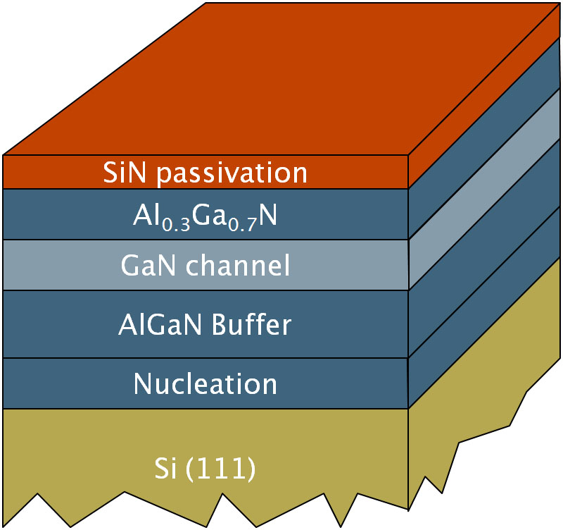
Figure 1: EpiGaN deposits a unique in-situ SiN capping layer, grown by MOCVD on top of HEMT epi wafers.
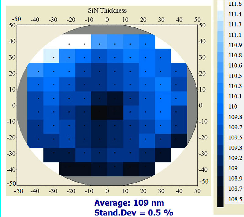
GaN appears to be a highly suitable material for power switching devices operating at high frequencies without suffering major losses. The Promise of GaN This is due to the drastically lower on-state resistance of GaN power transistors, combined with considerably reduced input and output capacitances. The higher switching frequency substantially reduces the volume of accompanying passive components such as inductors, transformers, and capacitors. Thus, a GaN-based power system is smaller and more lightweight than MOS- or IGBT-based systems. Eventually, GaN power electronics will combine these significantly improved operational properties with lower costs. Active components limit the efficiency of present systems. Converting GaN's potential into success hinges on scaling production to larger wafer sizes and employing appropriate passivation techniques. There is a tremendous opportunity for substantially lowering the energy losses associated with AC-DC and DC-DC conversion. If a new generation of devices can combine higher power levels with lower switching losses at higher operating frequencies, they will boost the efficiency of power systems, while trimming size and weight. Making Nitrides Affordable As wide-band-gap semiconductors, GaN-on-silicon devices belong to a superior class of materials: One of their biggest advantages is their high breakdown voltage, which stems from a breakdown field strength that is an order of magnitude higher than that of silicon. Due to the high carrier mobility and concentration associated with the 2DEG (two-dimensional electron gas) of the AlGaN/GaN heterostructure, nitride devices in switching applications also combine a low on-resistance with high switching speed. Additionally, their wide-band-gap properties enable them to operate at high temperatures. Development of nitride power devices has been underway for more than a decade, and their progress has enabled today's switching devices to outperform their silicon rivals. In the performance stakes, SiC is a tougher opponent, but GaN more than holds its own. GaN-on-silicon is the most cost-efficient wide-band-gap technology. It has developed to a point where it is feasible to deposit advanced heterostructures on silicon substrates up to 150 mm in diameter. In the near future, this will extend to 200 mm. There is also an opportunity to develop process compatibility with standard CMOS technology. This would open the door for further cost reduction by using existing lines at 200 mm silicon fabs operating around the globe. No wonder GaN power-electronics technology is attracting increasing interest. Until very recently, no one was able to achieve a real break-through—a reliable device operating at 600 V. This, however, is beginning to change. There have been demonstrations earlier this year of fully qualified 600 V GaN switches and they are slowly finding their way into commercial equipment. Cost, of course, is still an issue, but this reflects the typical learning curve that all novel technologies must undergo. One of the technical—and economic—challenges is to establish a compound-semiconductor technology in a field where silicon dominates. Although the performance of SiC diodes is attractive for power converter manufacturers, they are too pricey. In addition, until recently these diodes could not pair with SiC transistors, which had been detrimental to the uptake of this first-on-the-market wide-bandgap technology. For GaN technology to be commercially attractive, 600 V devices must be reliably producible on GaN-on-silicon epitaxial structures. Taking out the Strain EpiGaN's epitaxial growth process tackles the grid strain that arises in processes that deposit GaN on silicon. The two materials show different crystalline properties and thermal expansion coefficients. Left unchecked, this can lead to unchecked strain in the epi layer and substrate that can ultimately cause the wafer to bow and even crack. Carefully managing this strain yields wafers suitable for regular silicon processing lines. The company now routinely manufactures 150 mm epi wafers with a bow well below 50 μm—typically 20 to 30 μm, depending on wafer specs. Uniformity, in terms of standard deviation of either layer thickness or electrical characteristic, is typically better than 3%. The process optimizes these epi wafers for high-voltage high-frequency operation, which requires the formation of a buffer layer that withstands high voltages. This is because, in devices formed with high-quality GaN layers, the silicon substrate limits the upper breakdown voltage. EpiGaN's epi wafers for high-voltage devices show a buffer leakage current well below 1 μA/mm at 600 V. Operating frequencies above 100 GHz are possible due to the reduction of buffer traps. Stress engineering certainly is a challenging aspect of forming GaN-on-Si. Even more challenging is the passivation of surface states. A piezoelectric material, GaN has an excellent high-electron concentration associated with high electron mobility—obtained without extra doping. The price to pay is an extreme sensitivity governing device characteristics, such as current density and threshold voltage on the filling of those surface states, which have a density comparable to that found in the channel. If passivation is poor, the device's dynamic behaviour suffers. To combat this so-called dispersion problem, fabricators must process devices in a carefully controlled manner using high-quality epi wafers, because this leads to optimized buffers and controlled surface states. Uncontrolled charging or discharging of these surface states, which processing and device operation can modify, can severely degrade the device's dynamic properties. As a countermeasure, EpiGaN deposits a unique in-situ SiN capping layer, grown by MOCVD (metalorganic chemical vapour deposition ) as part of the epitaxy process on top of HEMT (high electron-mobility-transistor) epi wafers (Figure 1). The interface between this capping layer and the top nitride surface is incredibly smooth, and it enables excellent passivation of surface states.
Many processes use a GaN capping layer, which is less sensitive to the formation of these surface states than the AlGaN barrier in combination with PECVD (plasma-enhanced chemical vapor deposition) SiN that deposits after the MOCVD process as part of the device processing. However, this approach does not have the advantages of the in-situ deposited SiN. The capping layer can properly control surface-state filling during device operation. It is believed that SiN can provide enough charge to neutralize the surface charge of the AIGaN barrier layer so that its surface potential no longer contributes to 2DEG depletion. In addition, the SiN layer aids device stability at elevated temperatures. In-situ deposited SiN films can also lead to lower channel resistance. This enables adjusting the top part of the FET so that it can meet particular device specifications. GaN FETs are lateral devices, and optimizing their performance demands a trimming of conduction losses. This means that, for switching applications, aluminum-rich barriers are preferred in a typical AIGaN/GaN structure, because it yields a higher piezoelectric field, higher current density, and lower specific on resistance. One of the major benefits of the SiN cap layer is that it enables higher aluminum concentration without any significant material degradation. This is not the case in transistor structures with an uncapped or GaN-capped AlGaN/GaN 2DEG, where relaxation of the strained top AIGaN layer typically prevents high aluminum content in the top layer. For the SiN/AIN/AIGaN design, sheet resistance falls to 235 ?/? with appropriate passivation (Figure 2). For this structure, Hall measurements indicate that the electron sheet concentration is 2.15 x 1011 cm-2 and electron mobility is 1,250 cm2/Vs. These are very promising values and they enable the fabrication of devices with high transconductance, even when the gate length is relatively large. They highlight the potential of this device for high-frequency operation. The neutralization of surface charges provided by the SiN layer also unlocks the door to an innovative approach for making enhancement-mode devices. This form of transistor, which is generally preferred for power converters, can form by combining a thin AIGaN barrier layer with local removal of SiN under the gate. As for examples of the alternative use of depletion mode transistors, there are very few applications in practice. Using depletion mode devices generally means a work-around on the circuit level to separate the input side from the output side and ensure safe operation. One example thereof is the cascade configuration where a low voltage enhancement-mode Si MOSFET combines with a high-voltage GaN depletion-mode HEMT. From 600 V to 1.2 kV EpiGaN now makes GaN-on-silicon wafers with a breakdown voltage above 600 V and very low leakage current. This is by no means the upper limit, however. Recent work has yielded FETs with a breakdown above 2 kV. GaN is already used for power products in the 30 to 200 V, and 600 V range, and 1,200 V will soon be added. This will pave the way for replacing two silicon MOSFETs with a single GaN HEMT—trimming the cost and weight of power converters. Future products based on this process will complement the existing range of 4-inch and 150-mm epi wafers for high-voltage and high-frequency applications. Production capacity for these products is currently ramping up. In parallel, processes for 200 mm GaN epi wafers operating at 600 V and 1,200 V are developing. Larger wafer sizes will spur a cost reduction and enable GaN to deliver in a field where, until now, no compound semiconductor has seriously challenged silicon. EpiGan