Author:
Franz Stückler, Infineon Technologies
Date
07/05/2013
 PDF
PDF
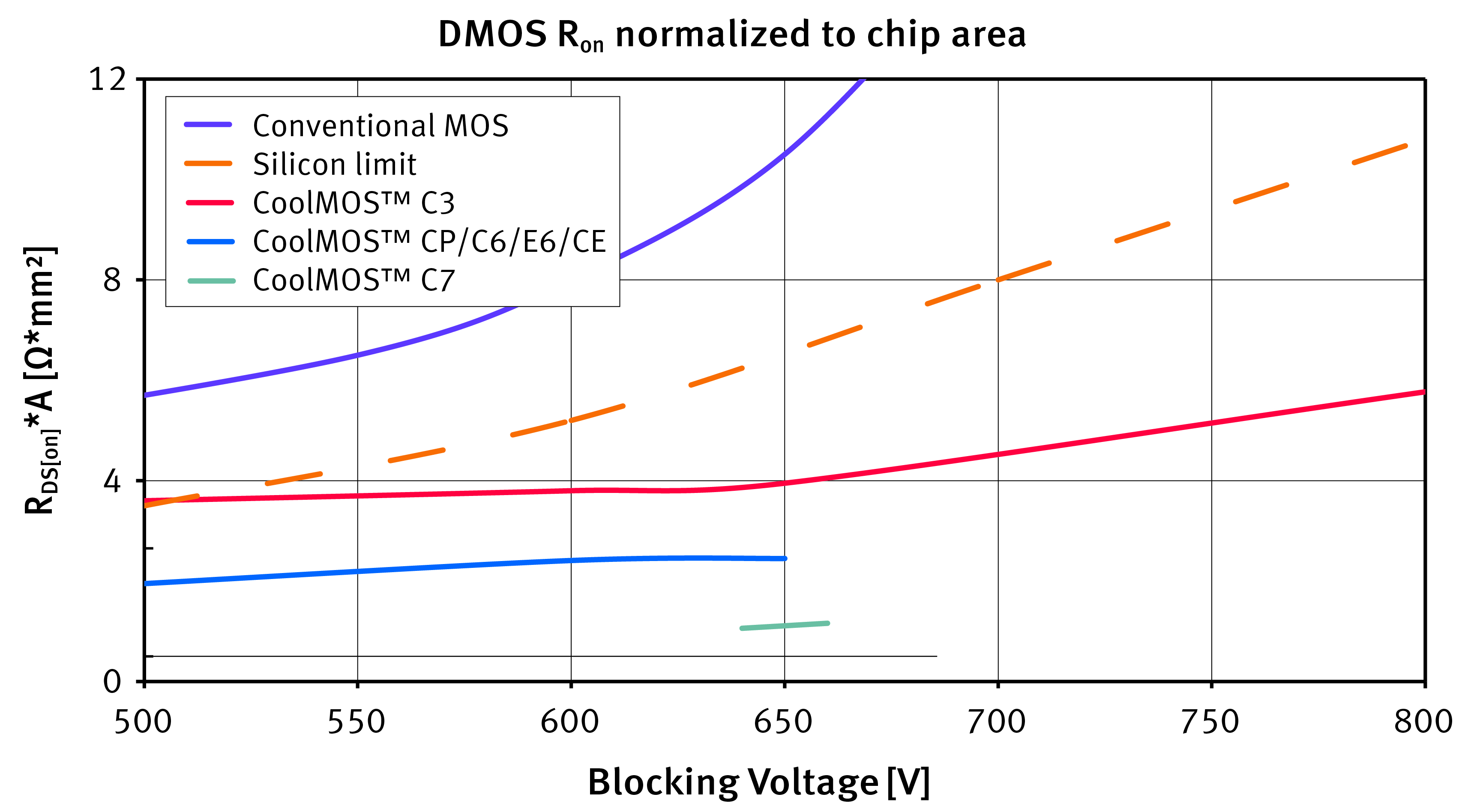
Figure 1
For more than a decade, development of Infineon's CoolMOS™ super-junction (SJ) MOSFET technology has extended the "silicon limit line" that restricts the performance of planar-type power MOSFETs. The steady advance is a result of continuing refinement of both transistor architecture and manufacturing process to balance area-specific conduction and switching losses. The latest CoolMOS C7 MOSFETs set new levels of performance for design of the highest-efficiency power supply and power conversion systems. Since the first commercial launch of CoolMOS SJ MOSFETs in 1998, Infineon has introduced two device families targeted at specific markets and several others intended for broad application in power switching. CoolMOS C7 is the latest technology for Best-in-Class performance in Power Factor Correction (PFC) and other hard switching topologies. It provides a significant reduction in device size and higher application performance than previous families. Comparison of several devices [Figure 1] illustrates how super-junction devices in general have re-defined the silicon limit line, and shows how the C7 series achieves area specific RDS(on) of less than 1 Ohm*mm2. With corresponding major reductions in device capacitances, all important Figure of Merit (FOM) indicators of C7 are incredibly low. To best leverage the outstanding performance characteristics of C7, power conversion designs need to account for the specific behaviors inherent to the technology. This article examines both the general behavior of SJ MOSFET devices and specific characteristics of C7 to provide guidance in selecting the best device for a given application.
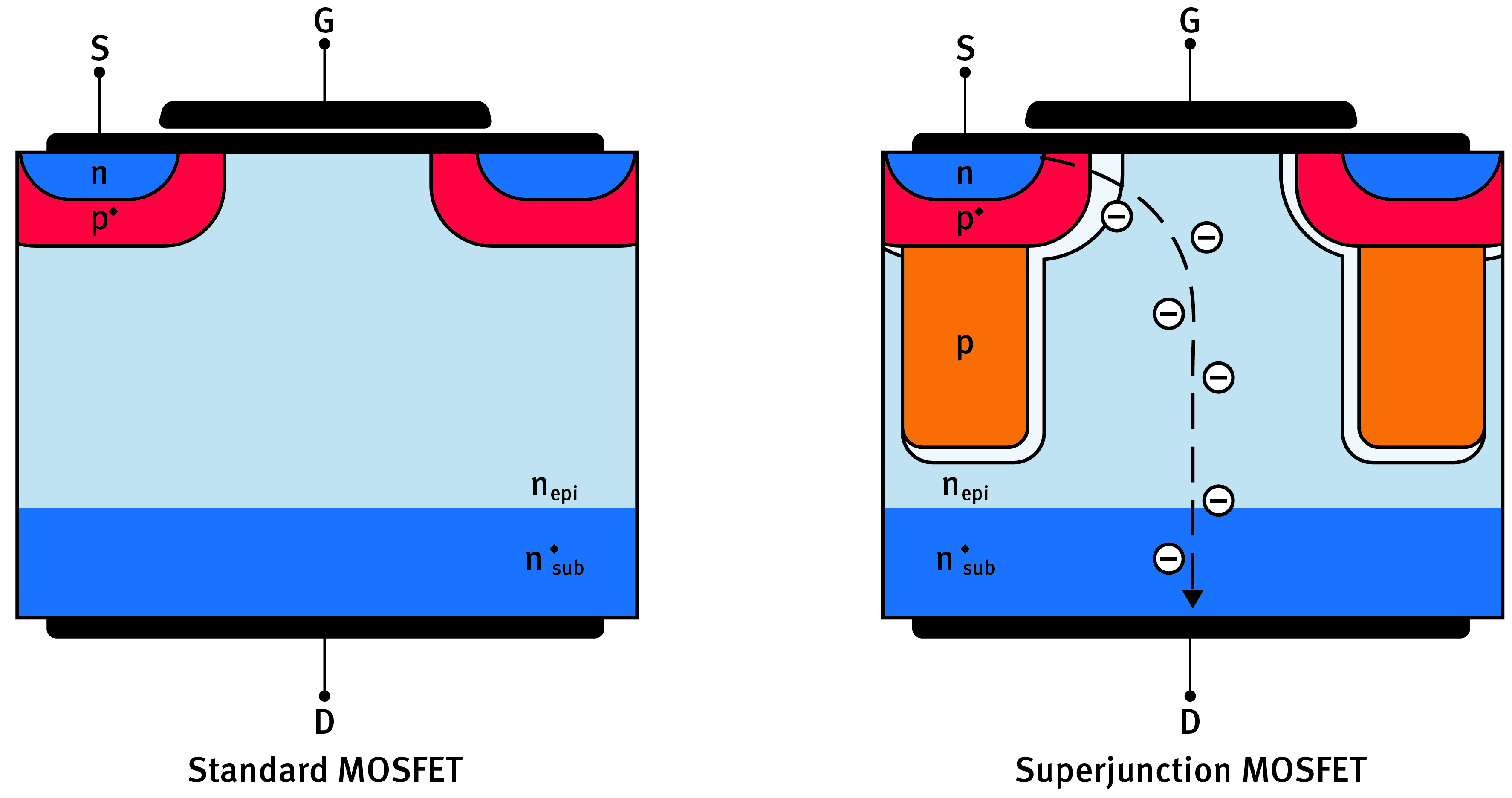
SJ MOSFET Characteristics In conventional high-voltage planar MOSFETs, about 95% of overall blocking voltage is in the drain drift region. [Figure 2] The limits of this blocking voltage are a function of thickness and doping. In a SJ MOSFET, the drain drift area is heavily doped to reduce the on-state resistance. P-doped columnar structures are added, and these columns and the n-doped regions are dimensioned to achieve high blocking voltage when the transistor is turned off. In its first generation, the dramatic reduction in area specific resistance of a super-junction MOSFET allowed a five-fold reduction in chip area compared to standard planar devices at that time, accompanied by lower capacitance and dynamic loss figures. These characteristics have been amplified in C7. Due to its balanced device structure, this seventh-generation SJ MOSFET delivers lowest switching loss times RDS(on) for hard switching topologies. The value of area-specific conduction and switching loss balance for high voltage transistors increases as designers seek higher power density through efficiency (lower losses) and higher switching frequencies (to reduce passive component size). While the balance between higher load currents, lower switching frequency and area specific loss shifts between different MOSFET technologies, better area-specific RDS(on) and lower capacitance, if used properly, will deliver the lowest losses in high density power systems.
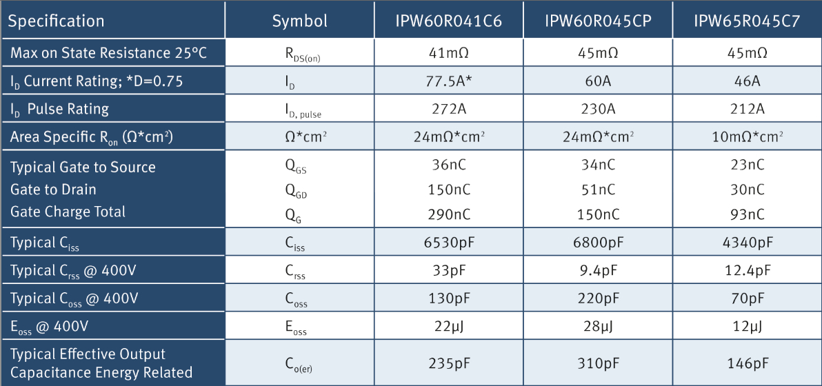
Super-junction MOSFETs also show a stronger nonlinearity of capacitance, due to the large area for the output capacitance at low voltage formed by the P-columns. As blocking voltage rises during switching, and the depletion region folded around the P-columns becomes a planar blocking region, Coss and Crss drop dramatically. This drop is even more pronounced with C7 CoolMO transistors and contributes to low switching losses, especially in hard switching applications. The combination of FOM improvement, very low gate charge, and low output capacitance makes it possible to switch at high voltages in just a few nanoseconds. For this reason, the dv/dt limit of C7 has been enhanced to 100V/ns compared to the standard 50V/ns of other SJ-MOSFET devices. A more detailed view of the electrical characteristics of three typical CoolMOS devices illustrates the advancements made in C7 [Table 1]. The most obvious change is the substantially improved area specific RDS(on) and the lower RDS(on) ratings now available in standard packages. Beside this obvious change the switching behavior has also changed for the much better.
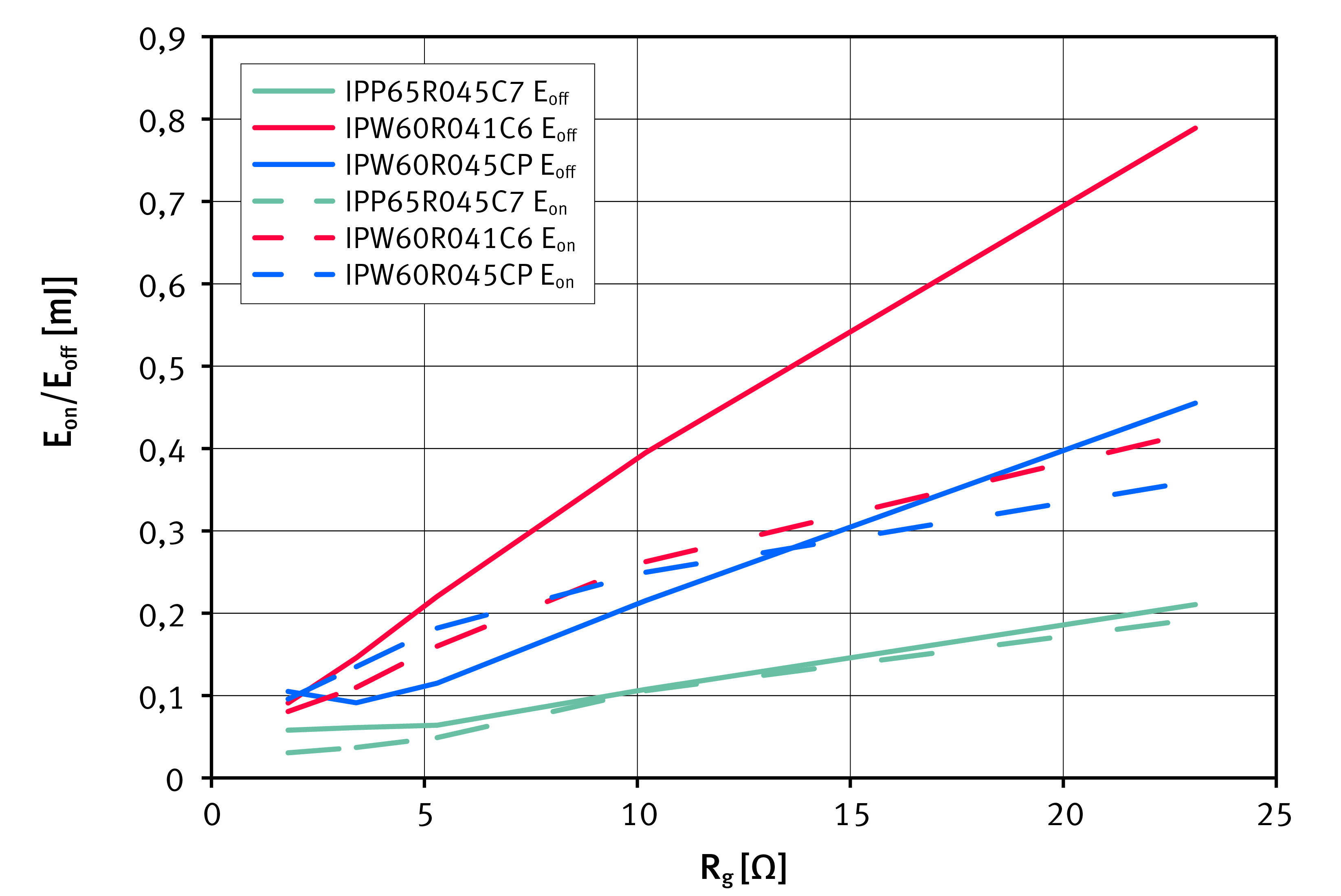
Due to the comparatively lower Coss at high voltage and faster switching for the gate drive, Eon and Eoff losses drop considerably for C7 compared with the C6 and CP devices. The results of Eon and Eoff characterization measurements for CoolMOS C7, CP, and C6 explain why. In tests made with 25A drain current load, VGS=12V, VDS=400V, and a range of gate resistor RG from 1.8 Ohms to 23 Ohms, there is the expected range of decreasing losses as a function of lower gate resistance. Interestingly, C7 also achieves losses under 0.1 ?J with resistance levels easily 10 times higher than for C6 due to the differences in Crss and total Qgd charge. CP also requires much lower RG to get in the range of comparable turn-off loss, and cannot match the turn-on loss of C7. [Figure 3]
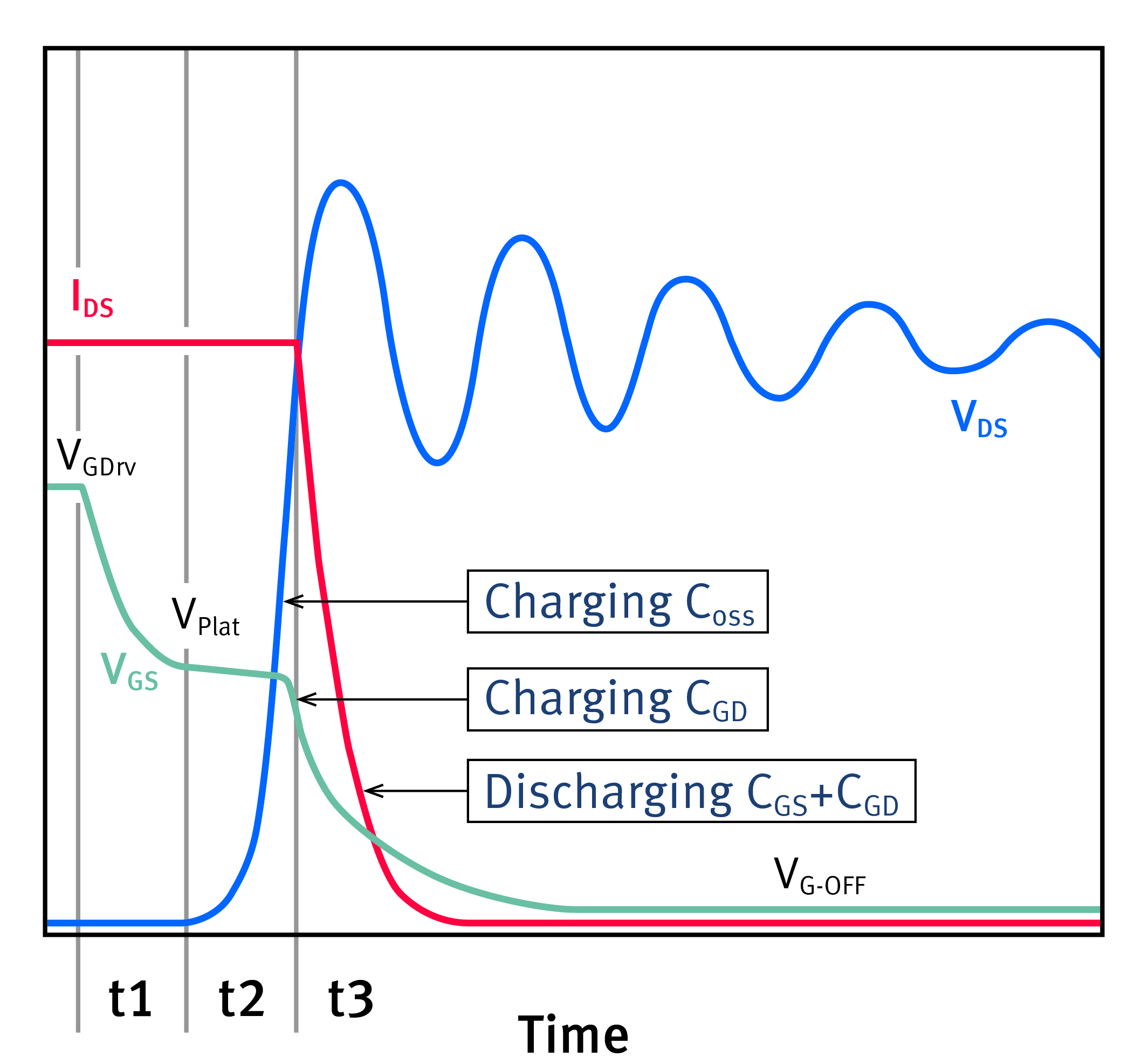
Dynamic Switching Application Considerations With the speed of C7, secondary effects such as package inductance and PCB parasitic inductance have increased impact on switching behavior. Turn-on behavior in particular is strongly influenced by the overall application circuit and associated components. Interestingly, turn-off behavior continues to be dominated by MOSFET characteristics, i.e., the interaction of internal and external gate resistance and capacitances. A simulation of turn-off behavior [Figure 4] displaying the gate input waveform, drain to source voltage, and drain current shows how the gate drive retains complete control over the dv/dt of the MOSFET, and is directly sizable by adjusting the size of the gate input resistor. However, as gate charge and Crss at high voltage become lower in MOSFETs and output capacitance non-linearity increases, using low values of gate drive resistance eventually shifts the switch-off behavior into a different mode.
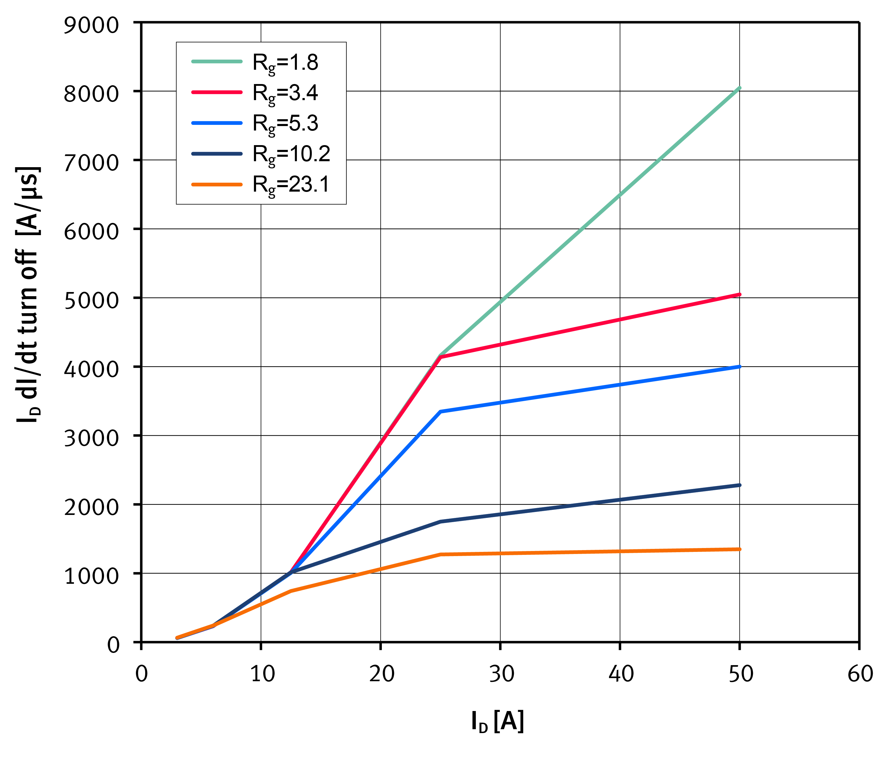
With very low values of gate driver resistance, di/dt is more under control of the surrounding circuit elements of the MOSFET [Figure 5]. For example, with a gate input resistor of 1.8 ? for an IPP65R045C7, di/dt rises quite rapidly with load current, until limited by external parasitic inductance. In this case di/dt quickly reaches thousands of amperes per microsecond. With the gate resistor raised to 5-10?, the situation moderates, and the rate of charging Cgs controls the di/dt independently of drain circuit loading, keeping peak di/dt in this case to a fast 2,000 - 3,000A/?sec. Under conditions in which the gate drive turn-off is very fast, in combination with a relatively high Coss, and drain to source voltage is below 50-60V, the switching behavior will be dominated by different mechanisms. Also, the drain switching voltage will not be controlled by the gate drive current, but by Coss and load current. This mode does result in very low turn-off losses, as might be expected, but it has some characteristics that must be controlled in certain applications, such as PFC boost converters, which can see a wide range of input current and brief but high overloads. A comparison of several device choices for a typical PFC design [Table 1] shows that it will be worthwhile to work though these issues to use the C7 technology, particularly if light load efficiency and low gate drive power are considerations, or using a smaller package with lower inductance like the TO-220 (IPP65R045C7) will benefit the design.
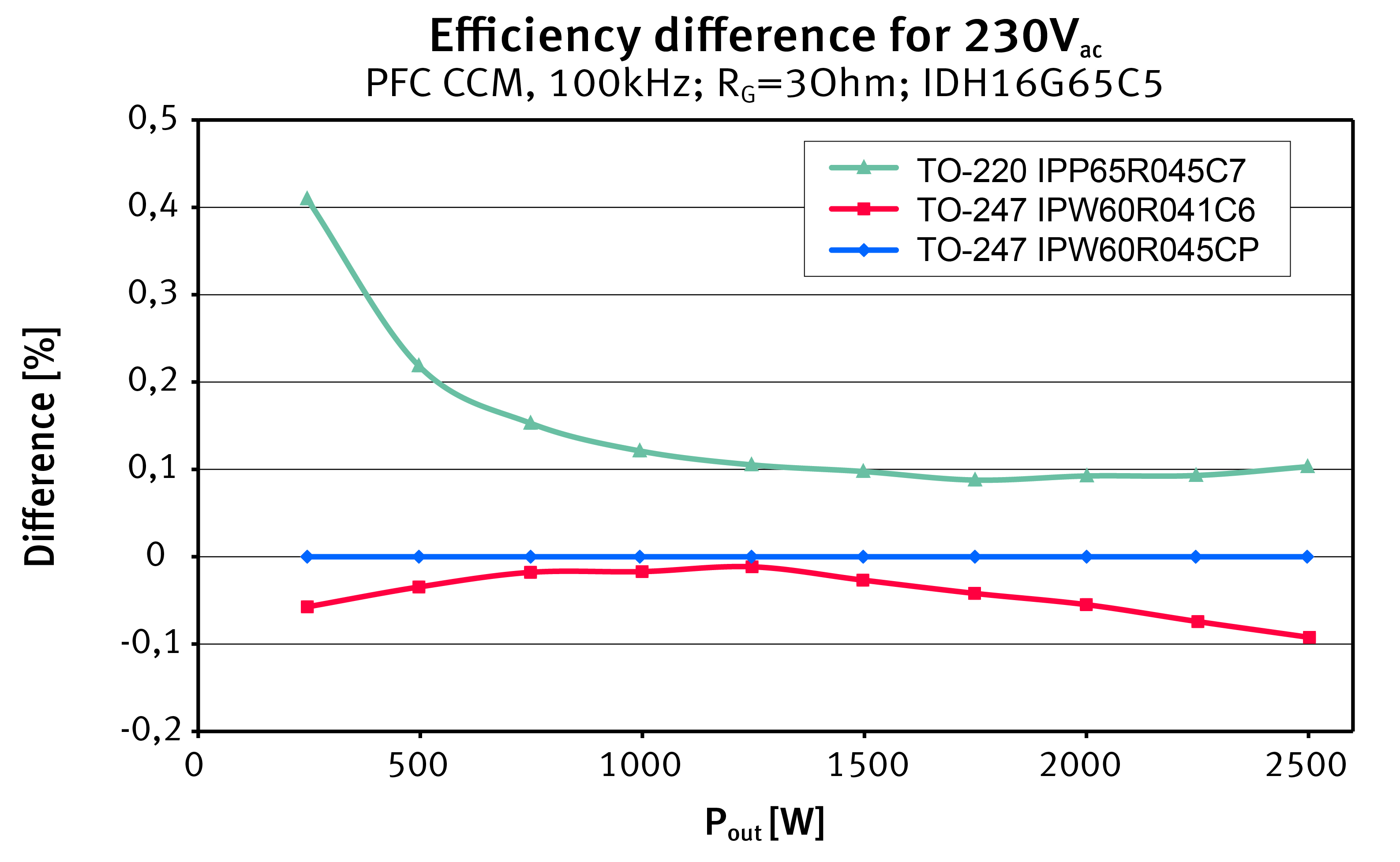
Figure 6 compares efficiency in PFC between the IPW60R045CP, the IPW60R041C6 and the IPP65R045C7, showing the efficiency differences normalized to that of the IPW60R045CP. The maximum output power of 2500W in this graph refers to the range where this class of MOSFET is used (typically 1800-2400W), and this plot would typically reveal differences in the area of efficiency peaking for the PFC converter at half power. Looking at the comparison of CP and C6, the differences arising from FOM (RDS(on)*QG and RDS(on)*Eoss) and switching loss approach a breakeven point at 1200W. At this power and output current, the FOM advantage of the IPW60R041C6 is swamped out by the lower switching losses for high current of the IPW60R045CP. Examining the IPP65R045C7 in comparison, a marked advantage in light load efficiency is seen due to the much lower Eoss loss and the generally better dynamic properties. At 1800W, it also maintains an advantage over both CP and C6. Although the temperature and therefore also the RDS(on) is increased for TO220 at 2500W, the IPP65R045C7 maintains efficiency due to the very low switching losses of C7-Technology. This effect is understandable, as the C7-Technology has much lower switching losses for same RDS(on), as shown in Figure 3. Therefore C7 is the enabler for increasing the frequencies without losing efficiency in the application. In the end, the optimum MOSFET selection for a specific application hinges on evaluation of factors specific both to the device and to the complete circuit and system design. With the launch of devices such as the CoolMOS C7 family, designers have greater flexibility to achieve the right balance of size and system efficiency. Infineon Technologies