Author:
Ron Lowman and Angela Raucher, Synopsys
Date
04/15/2016
 PDF
PDF
The Internet of Things (IoT) is providing increasing levels of transparency in our everyday energy usage, be it for connected factory equipment or small appliances or in exciting new market segments including wearables and drones. Advanced Power Management Integrated Circuit (PMIC) designs have implemented switched-mode power supply techniques for quite some time but greater efficiency requirements are driving more digital implementations to control these systems.
For system control, highly efficient processing of the math algorithms, fast response times and configurability are required. However, implementing advanced configurability within ICs to enable power system design is surprisingly inexpensive and less complex than prior perceptions may indicate.
Moving to the switcher
As linear power supplies transitioned to switched-mode power supplies, monitoring features were added, including an 8-bit processor or custom logic to react to potential over-voltage and over-current conditions. Switch-mode power supplies offer clear advantages over linear power supplies, but more control is needed to meet demand for higher efficiency power management.
The 8-bit processor for monitoring no longer suffices for future PMIC designs. The ability to control and configure the supplies is driving a migration to 32-bit ultra-low power processors with digital signal capabilities. Smart digital power conversion provides higher efficiency, which translates to longer battery life, smaller component sizes, and longer component life due to decreased wear and tear. Therefore, with the upgrade of processing capability there is a tremendous opportunity to conserve energy, improve system reliability, and ultimately lower system costs.
Digital control has currently been reserved for high-power applications that have very high dynamic loads due to the easily justifiable benefits. However, there is increasing focus on leveraging the benefits of these technologies in systems with lower dynamic loads. Full digital control of power conversion requires complex math such as Z-Domain math. To reduce costs and power, many compact 32-bit processors have a very reduced and limited set of fixed instructions, generally too reduced to even perform the math required by digital control of power conversion.
DSP instructions, which are required for these types of math algorithms, are typically the first instructions to be removed from the instruction set. This is where a solution such as the ultra-low-power DesignWare ARC EM processor can provide the ideal value proposition. For example, it is configurable to ensure the required instructions are available and has the ability to tightly couple peripherals and memory in a bus-less architecture minimizes area while delivering the required performance. Another advantage is industry-standard-based development tools to help manage the overall cost of ownership vs. traditional control implementations which use FPGAs or specialized digital signal processors and require the maintenance of a unique development environment and developers with very specific experience.
Choosing the right architecture
There is the additional concern of increased power consumption when moving to a higher performance processor, but this can also be mitigated with the right system architecture. For example, comparing the 8-bit and 32-bit subsystems in Figure 1, you can actually decrease dynamic power of the SoC current draw by 10X through tightly coupling the memory and peripherals and running at a low frequency to perform the same function.

Click image to enlarge
Figure 1. Comparison of an 8-bit processor-based subsystem and a 32-bit ARC-based subsystem
When focusing on battery-powered applications like wearables, energy consumption is also critical. It is important to select IP that minimizes total energy in the system. For example, some system architects might not think a higher performing processor is needed for a system. But, if that same processor can perform a function in fewer cycles, the overall energy can be reduced. Table 1 shows some key criteria related to energy consumption that need to be taken into account when selecting a 32-bit processor, and common ways to measure performance.
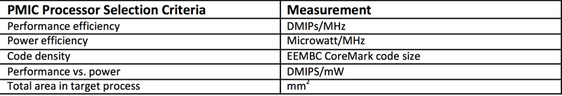
Most of the criteria are somewhat interrelated. Area affects power consumption and code density affects total area. One key thing to keep in mind is that the core area of the processor is not as relevant as the total combined area of the processor core, memory, and peripherals.
To implement smart power supplies capable of delivering intelligent control to increase efficiency, there are a few additional key IP blocks needed on the IC level beyond the discrete IGBTs, MOSFETs, and/or GAN transistors. They consist of a high-speed ADC, a flexible and high-speed PWM, a 32-bit compute engine capable of efficiently processing Z-Domain math, and some non-volatile memory (NVM) to store the necessary code. Much of the IP required to integrate everything into a single IC can be implemented as RTL in any process node, but there are some exceptions, such as the high-performance ADC and the NVM.
A high-performance ADC is needed within the system to respond to system changes, and for this ADC, a fast conversion rate is critical. As an analog block, it must be ported and tested in the desired process technology to verify the expected performance. For example, the Synopsys 5 Msps 12-bit SAR ADC is a leading general-purpose ADC and is available in a number of common IoT process nodes.
The NVM required for code storage is specific to the process technology. There are several NVM technologies that can be used for code storage including EEPROM, Flash, one-time programmable (OTP) and reprogrammable CMOS NVM. External EEPROM allows the most flexibility in terms of process technology but is not integrated and adds size and cost to the system. With flash you have the ability to reprogram the memory so updates can be made in development or in the field but there are two main drawbacks for integration in a PMIC. First, it is often costly, adding approximately 25% to the cost of wafers, and if you have a device dominated by analog/power transistors versus memory, then you are paying a penalty. Second, it is limited to certain processes and generally incompatible with technologies used for PMICs such as Bipolar CMOS DMOS (BCD).
One-time programmable memory is available in most process technologies and can be a solution for PMIC code, but the downside is that you cannot make updates to the code after you receive the silicon. Reprogammable CMOS NVM, such as Synopsys’ DesignWare Multi-Time Programmable (MTP) NVM IP allows you to reprogram the contents of the memory and update firmware in development and in the field and support BCD processes used commonly in PMIC design. The new Medium Density NVM IP offers flash-like functionality and extends the maximum memory size up to 256 kbits. Overall it is important to understand the tradeoffs for the system when selecting the NVM technology used.
The requirement to support multiple markets with the same silicon and address new markets such as IoT is driving the advancement of PMIC designs to support more digital control and programmability. There is an ongoing trend to transition from 8-bit to 32-bit processors that meet these requirements and it is critical to select the right processor and surrounding IP to minimize area and meet system level power goals. Synopsys’ ARC EM processors and DesignWare IP help designers to architect PMIC devices that have the future of power management in hand.