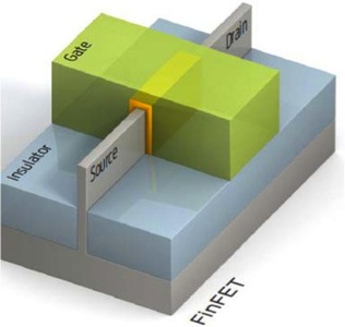
Synopsys, a global leader providing software, IP and services used to accelerate innovation in chips and electronic systems, today announced that its multi-year collaboration with Samsung on FinFET technology has achieved a critical milestone: the successful tapeout of the first test chip on Samsung's 14LPE process. While the FinFET process offers significant power and performance benefits compared to the traditional planar process, the move from two-dimensional transistors to three-dimensional transistors introduces several new IP and EDA tool challenges such as modeling. The multi-year collaboration delivered the foundational modeling technologies for 3D parasitic extraction, circuit simulation and physical design-rule support of FinFET devices. Synopsys' comprehensive solution for embedded memory, physical design, parasitic extraction, timing analysis and signoff is built on this foundation. "FinFET transistors can deliver lower power consumption and higher device performance, but they also bring tough challenges," said Dr. Kyu-Myung Choi, vice president of System LSI infrastructure design center, Device Solutions, Samsung Electronics. "We chose Synopsys as our FinFET collaboration partner to solve these challenges, because of our successful history together at 20 nanometer and other nodes. We continue to pool our expertise to deliver innovative FinFET solutions." Synopsys worked closely with Samsung to develop a test chip that validates Samsung's advanced 14-nm FinFET process as well as Synopsys' DesignWare Embedded Memories using Synopsys' Self-Test and Repair (STAR) Memory System® solution. The test chip will enable the correlation of the simulation models to the FinFET process and contains test structures, standard cells, a PLL and embedded SRAMs. The memory instances include high-density SRAMs designed to operate at very low voltages and high-speed SRAMs to validate the process performance. The shift from planar to FinFET-based 3D transistors is a significant change that requires close technical collaboration between tool developers, foundries and early adopters to deliver a strong solution. Synopsys' highly accurate modeling technology provides the foundation for the FinFET-ready Galaxy™ Implementation Platform. The platform includes IC Compiler™ physical design, IC Validator physical verification, StarRC™ parasitic extraction, SiliconSmart characterization, CustomSim™ and FineSim for FastSPICE simulation, and HSPICE® device modeling and circuit simulation. "Samsung is a key partner in our effort and investment to develop a complete solution for FinFET technology," said Antun Domic, senior vice president and general manager of Synopsys' Implementation Group. "Synopsys' extensive collaboration with Samsung enables us to deliver best-in-class technologies and IP to help designers realize the full potential of FinFET transistor designs." Synopsys Samsung
 PDF
PDF