Author:
Alfred Hesener Marketing Director - Europe Fairchild Semiconductor
Date
03/05/2012
 PDF
PDF
Click image to enlarge
Figure 1
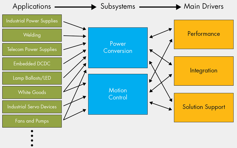
Power electronics subsystems are often divided in a control and a power circuit, where the power output stage components strongly determine the characteristics of the whole application, like efficiency, robustness or noise. Good alignment across the entire power stage subcircuit will enable higher performance, but also better robustness and larger design margins. For the gate driver, different choices like halfbridge drivers, optically isolated gate drivers or delay-matched lowside drivers will be compared against discrete solutions, and for the power stage the decision criteria for different power switch technologies are explained with practical examples. Finetuning the driver stage to the power switches plays an important role in the optimization process of the system. System trends in power electronics applications In all power electronics applications, two types of power subsystems can be found - power conversion and motion control circuits. The first may also be called AC/DC or power supply, the second can also be called inverter or frequency converter. Both benefit from the same three factors that are driving the development, namely performance of the components, increased integration, and solution or design support. Performance of the controllers, gate drivers and power switches is crucial for increasing performance. Improvements in efficiency in operation and standby power reduction can only be achieved with new technologies for the power switches, and new and improved features for the controllers, enabling not only better performance of existing topologies but also implementation of new topologies. One example is the increased use of quasi-resonant power supplies, enabled today e.g. by Fairchild's PWM controller FAN6300.
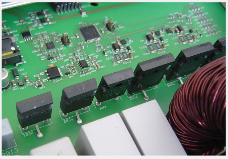
Efficient partitioning Optimizing the power output stage requires an in-depth analysis of the components and their performance characteristics, not only for pure performance values, like conduction or switching losses, but also regarding the integration with other devices. Without this optimization, larger design margins must be implemented, and no advantage can be taken from the use of more modern components. Power output stage examples In both subsystems mentioned above, power is being switched at a considerable frequency - for this article, we will not consider applications where switching is a result of a system status, e.g. line breakers, on/off switches or similar. Switching at a high frequency is desirable to reduce the size of the passive components needed, but at the same time switching losses are increasing. Higher frequency switching can also improve dynamic load transient behaviour, which may be a system advantage. In most cases, the power switches are not only connected to ground but also to the input, supply or "bus" voltage. Since these switches must be controlled with a proper gate drive voltage referenced to their source or emitter pin, a so-called "floating" driver is needed. This can be achieved through a junction-isolated driver, as in the case of monolithic gate drivers such as the FAN7080 from Fairchild, or through opto isolation, e.g. as in the FOD3120 from Fairchild. For motion control applications, it may be interesting to consider smart power modules, where the power switches are integrated with the gate drivers. Main advantages include higher reliability, better optimization of the components, smaller form factor, better design flexibility, and better protection features. In fact, the smart power modules demonstrate many of the advantages of a tight integration and alignment of the elements that are contained in the power output stage.
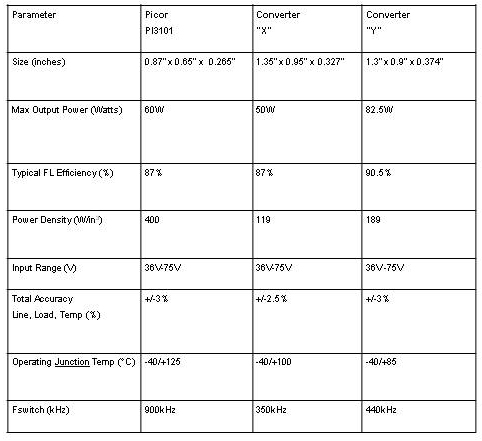
Selection criteria for the components The two most important factors influencing the choice of IGBTs as well as MOSFETs as main power switches are switching and conduction losses. The application will determine the maximum voltages and currents, and also the switching frequencies required. Table 1 illustrates the differences between the different switch technologies.
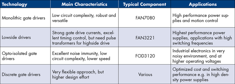
For driving the switches, specific gate drivers are being used, that can deliver large peak currents, e.g. up to 11A/12A (sink/source) in the case of Fairchild's FAN3222, and can securely "clamp" the gates when the switch shall remain in off-state. It is important to select the right gate driver peak current - higher currents may give no significant advantage in efficiency, but can cause large voltage overshoots in the system and difficult EMI behaviour, due to the fast edges that contain rich harmonic noise content. Three different gate driver families are available, the monolithic half bridge or high side gate drivers for most applications not requiring electrical isolation, the opto-isolated gate drivers with excellent noise immunities, and the low side driver family with excellent timing performance for higher-power applications, including pulse transformer drive. Table 2 illustrates the different gate driver families and their features.
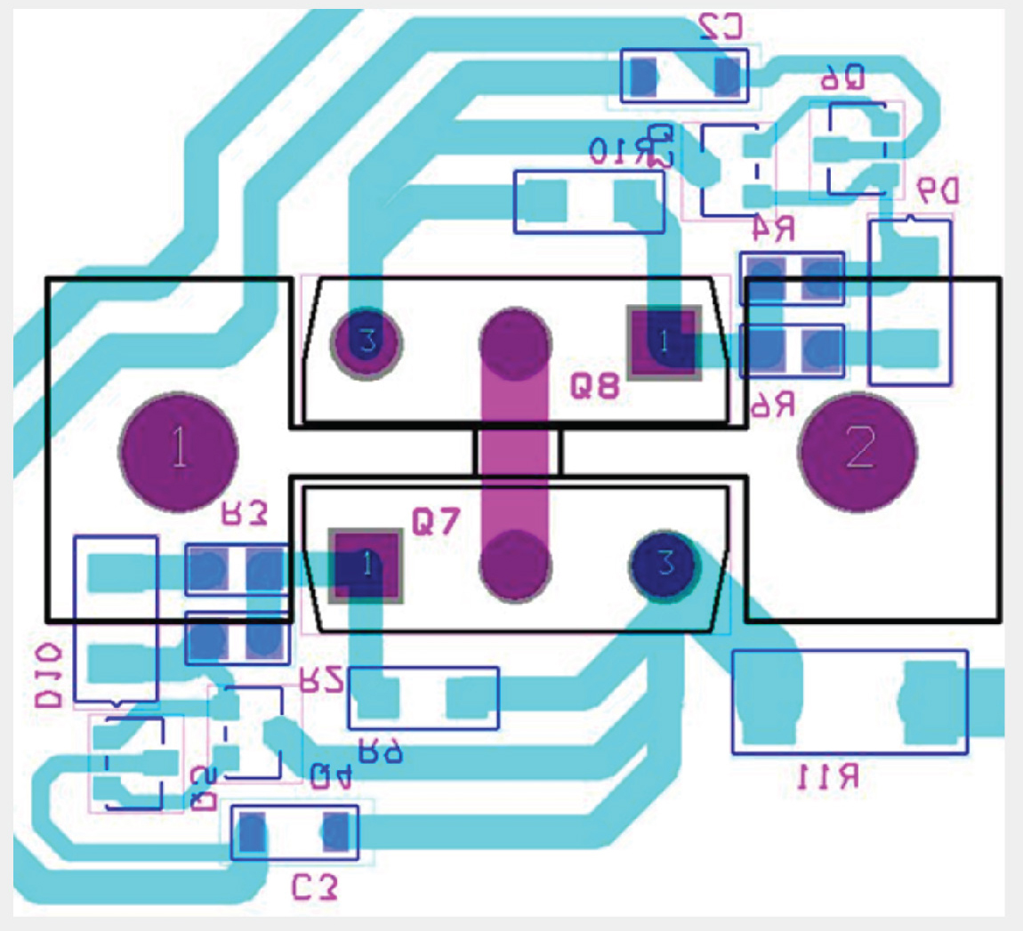
System level optimization The most important factors considered for optimization of the power output stage are of course power efficiency, impacting cost-of-ownership, but also size and cost, all impacted by the three key drivers. Looking beyond, more factors need to be considered in industrial electronics applications, in particular robustness (protection and continued operation in abnormal system states), but also reliability (operation without failure for extended lifetimes), and more severe environmental conditions. These additional requirements will mostly influence the thermal, electrical and layout design, with additional consideration needed regarding EMI behaviour. Figure 3 shows a power stage layout for a high density power supply, using parallel MOSFETs with both devices on the same heatsink. To improve the switching performance, the gate drive circuits (here with discrete components) are brought very close to the power switch they are controlling, in order to a) improve the gate drive current loop and make it as small as possible, b) reduce the parasitic gate-drain capacitance to prevent parasitic oscillations, c) bring the gate drive impedance as close to the gate as possible, again to prevent parasitic oscillations. Conclusion The optimization of the power output stage is complex, with many different choices that can be made at device level, but also many different requirements that may contradict each other. In this article the different technological choices have been illustrated, and optimization possibilities how to maximize the performance have been shown. It all depends on the fine-tuning of the power switches and gate drivers in the system, to achieve optimum "team play". www.fairchildsemi.com