Author:
Michael A. Briere, ACOO Enterprises LLC, under contract with International Rectifier
Date
04/15/2012
 PDF
PDF
Click image to enlarge
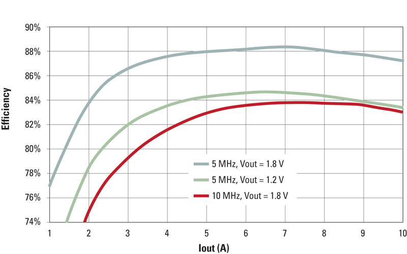
Figure 1 : Measured efficiency of a high frequency 12 Vin to POL buck converter, including output filter losses, using low voltage GaN based power devices.
There are relatively few opportunities in one's career to participate in the development of a truly revolutionary technology in a chosen field. The past 8 years have been such an opportunity for this author through the development of GaN based power devices. Over three and a half years ago, International Rectifier announced that it was working on a program, named GaNpowIR ���®, focused on the development of power devices for use in applications between 20 and 1200 V, based on the AlGaN-GaN high electron mobility transistor (HEMT), using cost effective hetero-epitaxy on silicon substrates and silicon CMOS foundry compatible device fabrication [1]. At the time, a projected time frame for the development of 600 V devices was the end of 2011. It is with a tremendous sense of pride in the accomplishment of the IR GaN team that this milestone was reached. Large area, high current devices were developed, meeting all performance criterion and have been provided to select OEM power supply partners for additional rigorous and independent application evaluation and further product definition refinement. Amongst the significant technical challenges that were met to achieve this goal of commercially viable 600 V capable GaN based power devices was the development of hetero-epitaxial techniques to provide reproducibly crack free, thick ( e.g. > 4.5 um) III-N epi on large diameter (150 mm) silicon wafers of standard thickness with resulting bow of less than 30 um. In addition, reduction of the drain to gate and drain to source leakage currents to below 1 nA/mm of gate periphery at the device rating of 600 V was achieved. The resulting devices exhibit an Ion/Ioff ratio of greater than 10 Million. Further, the essential elimination of transient charge trapping phenomena associated with such effects as drain current collapse and dynamic Rdson has also been accomplished. Finally, sufficient field engineering has been developed to provide long term reliability under applied drain bias stress, necessary to satisfy the rigorous commercial standards developed for silicon based incumbent devices. The 600 V application node is particularly important since it represents some 40 % of the entire market for power semiconductors between 20 and 1200 V [2], as well as an obvious performance to cost advantage of GaN based devices over the silicon incumbents, where the potential performance improvement is 10 to 100 fold [1]. Current social and economic emphasis on energy conservation is easily satisfied by the significantly improved circuit efficiencies as well as higher density and lower system costs achieved using such GaN based power devices in applications ranging from ac-dc power supplies, inverters for photovoltaics and motor drives for appliances as well as in primary and auxiliary power converters in electric vehicles. It is likely for this reason that the advent of commercially viable 600 V devices has received considerably more attention than that of the low voltage device developments provided in functional block, buck regulator power stage modules, as announced in early 2010. It is, however, the author's present contention that the low voltage GaN based solutions will have a significant impact on both the power semiconductor market place and the associated computing applications within the next 5 years. The significance is due, in part, to the fact that 20-40 V switch applications also represent some 40 % of the previously mentioned targeted total power semiconductor market between 20 and 1200 V [2]. In addition, this author argues that only GaN based devices offer the potential for efficient ( > 88 %) single stage compact conversion ( 12 Vin to 1.2 Vout) which will be required to effectively support future many core (> 32) micro-processor architectures, using conversion switching frequencies of greater than 30-50 MHz [3]. The present results using first generation commercial low voltage devices (RonQg = 30 mohm nC) in a 12 Vin to POL Vout converter are shown in Figure 1. Here it can be seen that excellent efficiency response of 88% is found across a wide load range at 5 MHz for Vout of 1.8 V and a record performance of 84 % efficiency is achieved at 10 MHz. As discussed previously [3] while silicon based devices, with a technological RonQsw limit of more than 20 mohm nC, are physically limited to about 3 MHz for a 12V to 1 V conversion with 88% efficiency, it is possible for GaN based HEMTs to support efficient switching, with these criteria, to > 30 MHz. In fact the current goal is to achieve 2 to 3 mohm nC performance, a factor of about 4 more than the calculated technological limit, within the next 5 years.
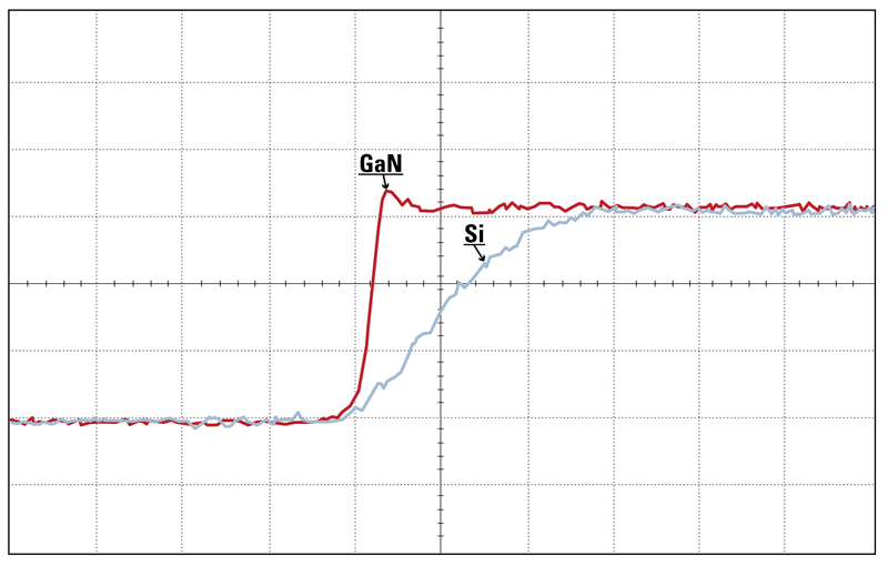
The mid-voltage power device market, for commercial application from 60 to 250 V, is highly fragmented and represents only some 10 % of the target market for power semiconductors [2]. For this reason, it has received less attention than either the 20 to 40 V or the 600 V rated device development activities. Even so, there are remarkable advantages for GaN based devices over silicon incumbents in this voltage application regime. One example is the class-D audio amplifier application with bus voltages of 60 to 100 V. In this bus range, 100 to 150 V rated devices are most often used in symmetric half bridge topologies. Exhibiting considerably less ( e.g. 40 % less in first generation devices) output charge, GaN based devices switch much faster than comparably rated silicon based devices, as shown in Figure 2 for a +/- 35 V bus and 100 V rated devices. Consequently the fidelity of the amplified PWM signal is far superior.
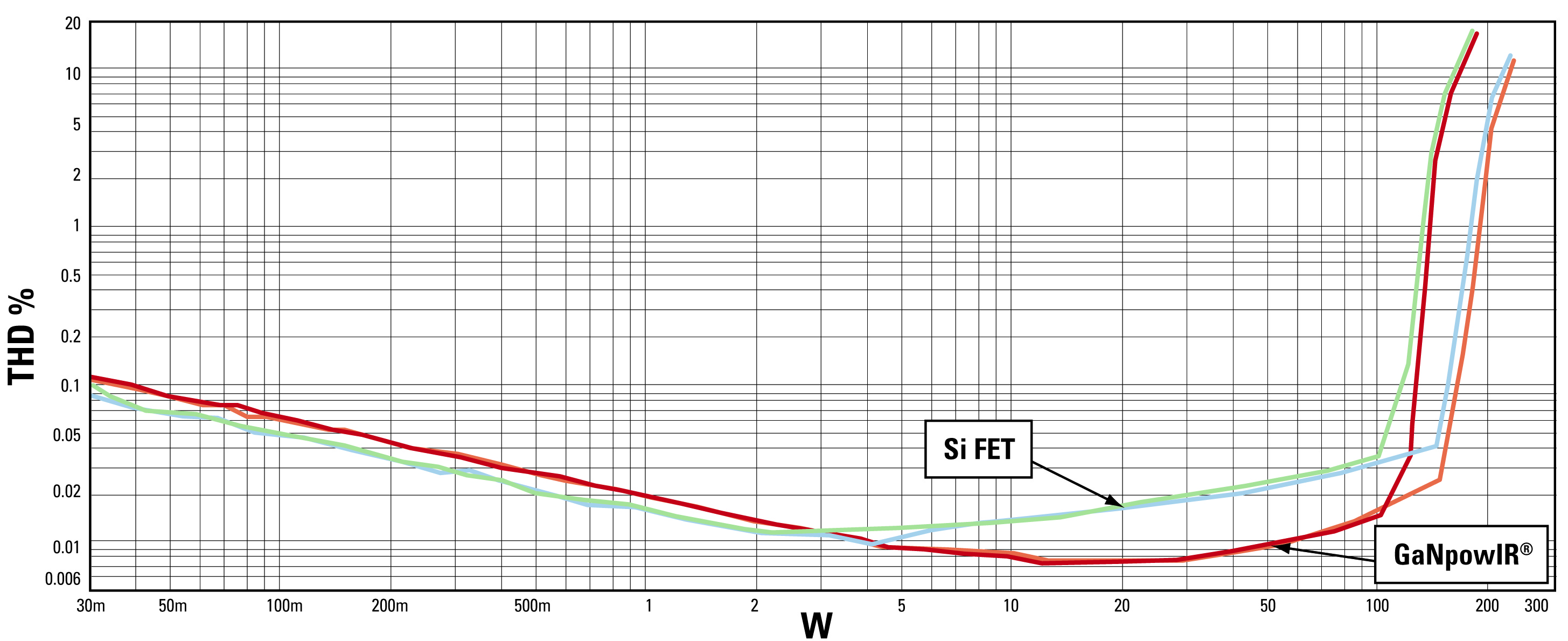
Shown in Figure 3 is a measure of the amplifier fidelity in total harmonic distortion across the applicable spectrum. As can be seen, the GaN based amplifier provides superior audio fidelity compared to the best in class silicon alternative. In addition, the GaN based solution provides improved power conversion efficiency across the entire load range of between 1.6 % at light load and more than 1 % at full load. In this case, despite the fact that these early GaN based devices are housed in a thermally inferior package, compared to the silicon devices which leverage the thermally optimal DirectFET���® package, the GaN solution is more than 10 C cooler at the operational load ( 1/8 clipping). In its first generation, IR's 600 V rated GaN based switches exhibit a factor of four improvement in conduction loss * switching loss performance, compared to best in class 600 V rated silicon based superjunction FETs as well as state of the art trench Insulated Gate Bipolar Transistors (tIGBTs). As in the case of the mid voltage devices, IR's 600 V rated switches are constructed as a two component cascode composite device. The first component, the native depletion mode GaN HEMT, is arranged in series with a low voltage silicon MOSFET, where the source of the silicon device is connected to the gate of the GaN HEMT and the source of the GaN HEMT is intimately connected to the drain of the silicon MOSFET. In this way, the inverse of the voltage developed across the silicon device is presented across the gate-source terminals of the HEMT. Amongst the many advantages of this compound device configuration is the freedom to drive the resulting switch in the same manner as more than 30 years of experience in driving silicon switches has made the circuit designer accustomed. Therefore, standard drive circuitry can be used and threshold voltages can be selected as required for the circuit environment ( e.g. from logic level to +4.5 V, as commonly used in industrial or very noisy circuit environments). As has been discussed previously [1], a GaN based 600 V rectifier can be similarly constructed by substituting a low voltage silicon diode instead of the FET. Since the wide bandgap III-N material has few minority carriers to effect switching behavior, the resulting rectifier behaves very much like a SiC diode, where the small reverse recovery charge is dominated by essentially temperature independent capacitive contributions. The low voltage silicon diode contributes only a small percentage to the total reverse recovery behavior. In this way, high performance rectifiers are possible at a fraction of the current SiC diode costs. This composite switch changes state very fast, since the GaN has a high transconductance ( e.g. 300 mS/mm gate width) and the effective GaN gate drive on-resistance is that of the silicon companion device (e.g. mohms). It is important to take adequate care of the potential parasitic inductances, present both within the switch packaged assembly and in the surrounding circuit layout, so as to effectively minimize ringing often associated with very fast switching. Demonstrating excellent device robustness beyond the nominal device dc bus rating of 480 V, such devices exhibit very clean switching behavior from a 600V dc bus despite greater than 50 V/ns transition rate for a packaged cascade switch in a power factor correction application circuit. Similarly clean waveforms have been found for transition rates approaching 100 V/ns for nominally rated 430 V bus voltages.
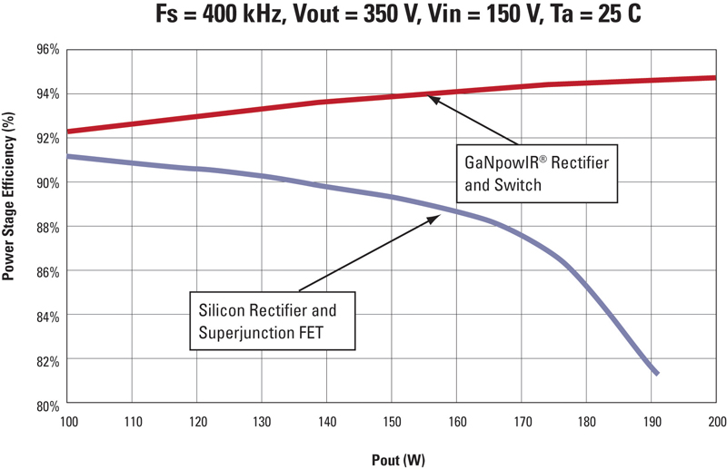
The fast transition rates allow for significant reductions in the switching losses using GaN based cascade switches. This can be seen in Figure 4, showing the efficiency improvement for GaN based switches and rectifiers in a nominally 200 W power factor correction boost circuit ( 150 Vin to 350 Vout) operating at 400 kHz, used in the front end of an ac-dc power converter, compared to the case of a state of the art silicon based superjunction FET and fast recovery diode used in the same circuit. As is well known, the higher operating frequency allows for significant reduction in the size and cost of the output filter L and C components, providing for a much higher density and lighter weight converter.
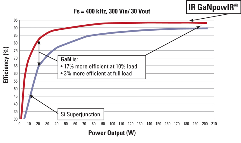
Another example of the advantages of using GaN based devices is shown in Figure 5, where the efficiency of a resonant LLC converter of 300 Vin to 30 Vout is operated at 400 kHz using either GaN based switches on both the primary and secondary side of the transformer, or best in class silicon alternatives. As can be seen, there is significant gain in conversion efficiency at both light ( 17 %) and full ( 3 %) loads. Such dramatic improvements in circuit efficiency and density are of course only modest examples of the potential impact of GaN based power devices on the power electronics industry. As it is expected that at least a further ten fold improvement in the performance characteristics of these devices are possible, revolutionary advances are expected in the future. Though this will most likely begin through the straightforward substitution of silicon incumbents with GaN based devices, the truly radical advances will occur when circuit topologies are designed specifically to take advantage of the unique attributes of the GaN based power devices. Besides the relatively ideal switching characteristics, recognition of the advantages of the inherently bi-directional nature of the GaN HEMT, the linear scalability of performance with voltage rating, as well as the inherent integratability of GaN based power devices will promote new architectures previously considered impractical, if previously considered at all. Given the cost effectiveness of the integratable GaN-on-Si technology platform, it is conceivable that future power conversion circuits will involve hundreds of power devices, instead of the current few. It is certainly an exciting time to be involved in the power electronics industry. [1] please see articles provided at www.irf.com/ganpowir [2] IHS iSupply 2011 [3] M.A. Briere, "Advanced Power Devices for Many Core Processor Power Supplies", IEDM 2010 session 13.6 www.irf.com