Author:
Edgar C. Taculog, TT Electronics
Date
04/17/2016
 PDF
PDF
Transformers can often provide an inexpensive solution for a variety of applications. The purpose of the transformer is to isolate the secondary side of the circuit from the primary power source, transfer power efficiently from the electrical source to the target load and protect users from hazards like electric shock, fire and heat.
The flyback transformer, which is an isolated version of a buck-boost transformer, does not in truth contain a transformer but a coupled inductor arrangement. When the transistor is turned on, current builds up in the primary and energy is stored in the core, this energy is then released to the output circuit through the secondary when the switch is turned off. The basic concept of this scenario can result in significant heat generation if not properly addressed (see Figure 1).
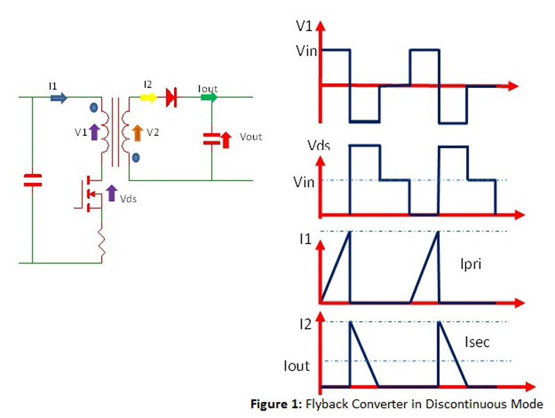
Click image to enlarge
Figure 1: Flyback Converter in Discontinuous Mode
Dewvices such as the HA00-10043ALFTR and HA00-14013LFTR line of transformers are designed specifically for use with Avago’s ACPL-32JT and ACPL-302J optocoupler ICs for automotive and industrial application respectively. The Avago devices are specifically used in a wide variety of applications that require high galvanic isolation so in designing these transformers materials that can meet the necessary creepage and clearance distances between conductors were taken into consideration. Likewise, the use of materials that can meet the UL94 V-0 flammability specification and a mechanical design able to withstand unintended drops and impacts are important.
Isolation requirements
Safety isolation requirements impose minimum dimensional limits for creepage and insulation thickness, which can waste a high percentage of a transformer core’s winding window area, especially in a small transformer. A bobbin also reduces the area available for windings. Triple insulated wire satisfies the insulation thickness requirement and eliminates the creepage requirement and is worth considering, especially for small transformers where creepage distances take up a large percentage of the window area.
Adequate isolation between power source and load, following SELV (safety extra-low voltage) circuit design principles, ensures equipment safety and protects operators from contact with high voltage circuits. TT Electronics’ HA00-10043ALFTR and HA00-14013LFTR transformers comply with regulatory safety requirements as stipulated for use with Avago’s ACPL-32JT and ACPL-302J devices.
The ACPL-32JT and ACPL-302J ICs are highly integrated power control devices that incorporate all the necessary components for a complete, isolated IGBT gate drive circuit. They feature a flyback controller for isolated DC-DC conversion, a high-current gate-driver, Miller current clamping, IGBT desaturation, and under-voltage lock-out (UVLO) protection with feedback (see Figure 2).
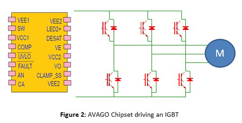
Click image to enlarge
Figure 2: AVAGO Chipset driving a 3-phase motor
Theory of operation
Successfully implementing an isolated power supply is perhaps most critically dependent on the specification and design of its transformer. There are many factors that impact the design: cost, size, heat dissipation, and material selection. In addition to the usual list of requirements dealing with high frequency isolated power supply transformer design, the following points should be carefully considered as well.
-Primary Inductance
-Turns Ratio
-Leakage Inductance
-Secondary Inductance
-Bias Current
-Winding Technique
-Target Application
Typically, the transformer turns ratio is chosen to maximize available output power. For low output voltages, an N:1 turns ratio can be used with multiple primary windings relative to the secondary to maximize the transformer’s current gain (and output power). However, the SW (switch output) pin on the Avago device will see a voltage that is equal to the maximum input supply voltage plus the output voltage multiplied by the turns ratio.
Together these conditions place an upper limit on the turns ratio for a given application. For lower output power levels, a 1:1 or 1:N transformer can be chosen for the absolute smallest transformer size. A 1:N transformer will minimize the magnetizing inductance (and minimize size), but will also limit the available output power. A higher 1:N turns ratio makes it possible to have very high output voltages without exceeding the breakdown voltage of the internal power switch.
There are no hard and fast rules to follow in establishing the optimum number of turns for each winding, but there are some general guidelines. An experienced magnetics engineer will first define the ideal turns ratios between windings to achieve the desired output voltages with a normal VIN* Duty Cycle.
When a specific core has been selected, the turns ratios will allow the actual number of turns to be calculated but unfortunately the results do not always provide the integral numbers required in practice. In such instances, a trial and error approach may be necessary, until the best compromise with integral turns is reached.
Looking at the ACPL-32JT/302J chips, we can see they operate from a nominal input voltage of 12VDC to produce a regulated output of 20VDC. The chipset primary side is powered directly from the source supply rather than from a bias winding within the transformer while the secondary side of the transformer powers the secondary side. The flyback configuration of 1:2 turns ratio results in an output voltage equal to 2*Vin, with the output voltage providing proper biasing for the chipset secondary side. Inside the chipset is an integrated switch that also limits the primary current using a sense resistor (see Figure 3).
![]()
Click image to enlarge
Figure 3. Switch Transition, Discontinuous Mode
Transformer leakage inductance (on either the primary or secondary) causes a voltage spike to appear at the primary after the output switch turns off. This spike is increasingly prominent at higher load currents where more stored energy must be dissipated. In most cases, a snubber will be required to avoid overvoltage breakdown at the switch node. To better protect the switching element, it is better to use snubbers to smoothen these generated spikes either using a passive RC network or a Zener diode combination if a more precise clamping level is needed (see Figure 4). Transformer leakage inductance can be minimized by good design practice but is often neglected under the pressure of achieving a faster time to market.
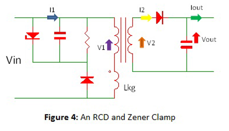
Click image to enlarge
Figure 4. An RCD and Zener Clamp
Leakage inductance on the secondary in particular exhibits an additional phenomenon. It forms an inductive divider on the transformer secondary that effectively reduces the size of the primary-referred flyback. This will increase the output voltage target by a similar percentage. Note that unlike leakage spike behavior, this phenomenon is load independent.
The primary current also circulates through the leakage inductance and causes an additional reverse voltage that adds to the previous one. If a RCD snubber is used, the clipping diode is forward biased and routes some current to the clamp network, transforming leakage energy into heat. Unfortunately, this leakage path also causes some of the energy stored in the gap to be transformed into heat.
In other words, any current flowing in the leakage inductance forces the same current to flow through the mutual inductance. Furthermore, the leakage inductance delays the primary to secondary energy transfer until its current has dropped to zero. This parasitic inductance also diverts a substantial amount of the stored energy, impacting the open−loop gain and requiring a higher primary current that in turn will require the design of a larger core transformer (see Figure 5).
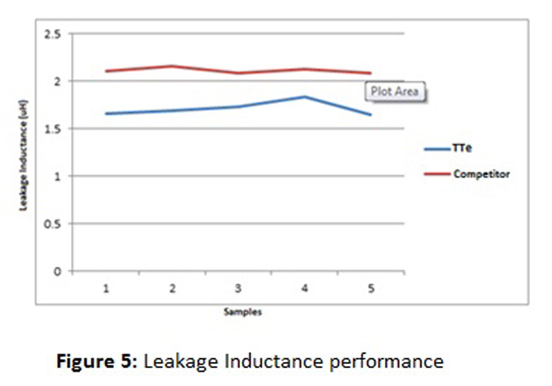
Click image to enlarge
Figure 5: Leakage Inductance performance
When the switch is closed, input energy is stored in the core’s gap with the total energy involved defined as: Energy stored = 1/2 Ipeak^2* Lpeak. But when the switch opens, the voltage across the primary inductance reverses and the primary/secondary energy transfer should occur immediately.
It takes a finite time until the transformer primary-side voltage approximately equals the output voltage. This is partly due to the rise time on the SW node, but more importantly is due to the transformer leakage inductance. The latter causes a very fast voltage spike on the primary-side of the transformer that is not directly related to output voltage. The leakage inductance spike is largest when the power switch current is highest.
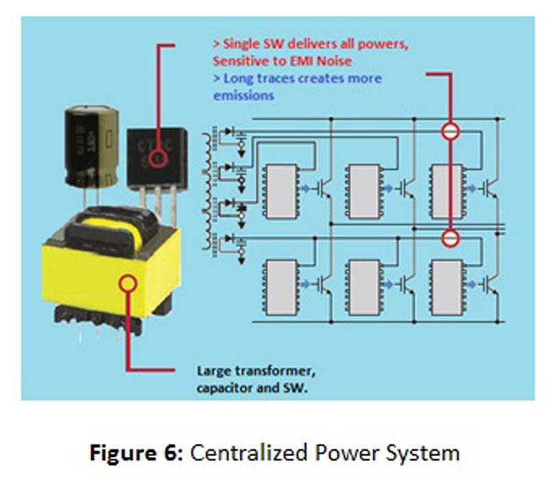
When circuit board space is limited, especially in automotive applications, there are trade-offs in designing a bigger transformer - between better electrical but inferior EMI performance. For higher turns ratios, a transformer with a larger physical size is needed to deliver additional current and provide a large enough inductance value to ensure that the off-time is long enough to accurately measure the output voltage.
Generally, the designer needs to determine if a centralized transformer design that requires a larger PCB board (see Figure 6) is better than using a distributed architecture where each transformer will require its own driver circuits (see Figure 7). A larger transformer must operate at a lower power density because, as its size increases, the surface area for dissipating heat it proportionately less than its heat-producing volume.
Click image to enlarge
Figure 6: Centralized Power System
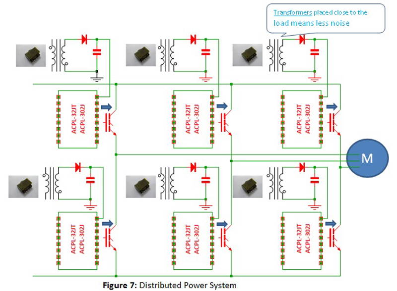
Figure 7: Distributed Power System
Aspects of actual transformer design and performance will be considered in the next part of this article.