Notable & Newsworthy

October 2015
Mouser and Grant Imahara drive innovation with

Back to the Future Day contest

Mouser Electronics, an authorized distributor with the latest semiconductors and electronic components, is teaming up with celebrity engineer Grant Imahara to announce a new social media contest to support the upcoming Back to the Future Day on October 21, 2015. Mouser is asking the engineering community to ei
. . . Learn More
Date:
10/20/2015

Graphene: controlling absorption

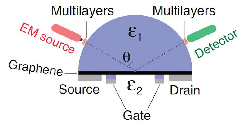
A practical EM wave-switching device in which the two dielectrics surrounding the graphene would be silicon and a vacuum, and the electron energy could be tuned using voltage gates

Flat sheets of graphite just one carbon atom thick, called graphene, display unique optical and electronic properties for use in future devices. In particular, graphene is nearly transparent to light and other electromagnetic (EM) waves, making it useful for liquid crystal displays and light-emitting diodes. Ho
. . . Learn More
Date:
10/08/2015
Liquid cooling moves onto the chip for denser electronics

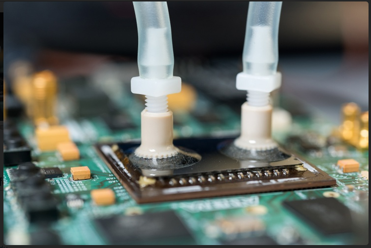
Liquid ports carry cooling water to specially designed passages etched into the backs of FPGA devices to provide more effective cooling.

Using microfluidic passages cut directly into the backsides of production field-programmable gate array (FPGA) devices, Georgia Institute of Technology researchers are putting liquid cooling right where it’s needed the most – a few hundred microns away from where the transistors are operating. Combined with conn
. . . Learn More
Date:
10/08/2015
Tunnel transistor may meet power needs of future chips

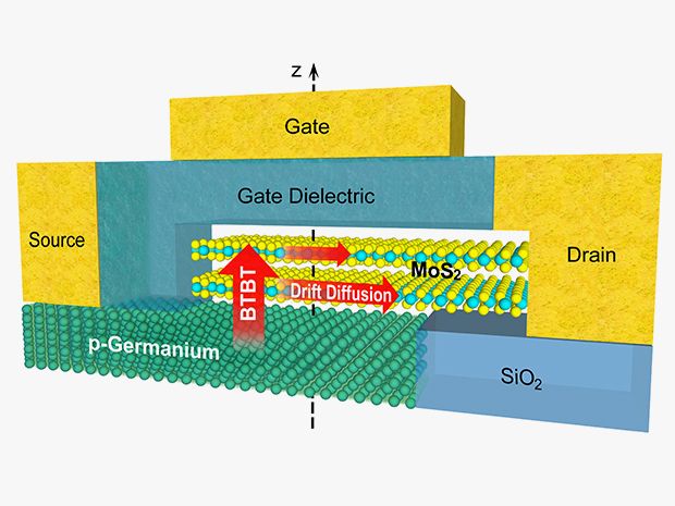
Schematic diagram illustrating the cross-sectional view of the ATLAS-TFET with ultra-thin bilayer MoS2 (1.3 nm) as the channel and degenerately doped p-type Ge as the source. Path for electron transport is shown by the red arrows, which run vertically (indicating band-to-band-tunnelling, BTBT) from the Ge source to the MoS2 and then laterally through the MoS2 layers (via drift diffusion) to the drain. As the Ge is highly doped, the tunnelling barrier height is mainly determined by the effective band overlap between Ge and MoS2 while the tunnelling width is determined by the MoS2 thickness (including the van der Waals gap).

A new kind of transistor consumes 90 percent less power than conventional transistors, dramatically exceeding a theoretical limit for electronics, researchers say. These findings could one day lead to super-dense low-power circuits as well as ultra-sensitive biosensors and gas sensors, the investigators added. The relentles
. . . Learn More
Date:
10/08/2015
Archives


-->