Author:
Dr. Ray Ridley, President, Ridley Engineering
Date
10/15/2014
 PDF
PDF
In this article, the loop gain of the five-output forward converter is measured and compared to predictions. The final loop design is compensated with a combination of theoretical design and empirical measurements, resulting in a Type I compensator for optimal results.
Measuring the Loop of a Five-Output Forward
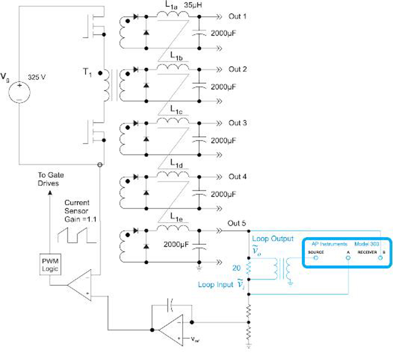
Figure 1 shows a five-output forward converter with coupled inductors. In the last article of this series, the control-to-output transfer function was measured, and found to have significant differences when compared to the predictions. The discrepancies were due to the coupled-output structure of the converter, and parasitics of the magnetics. This leads to measurement results that can be difficult to predict.
After measuring the control-to-output transfer function, the compensation was designed, and the control loop was measured as shown in Figure 1. The loop was closed and measured on the 12 V output of the power supply. Normally, a Type II amplifier would be used for a current-mode control loop. However, the characteristics of the coupled-inductor design provide an area of increasing gain in the control-to-output transfer function with a corresponding phase lead. This allows us to use a simple integrator, or Type I compensation.
Click image to enlarge
Figure 1: Forward Converter with Five Coupled-Inductor Outputs. Loop Gain Measured with the AP300 Analyzer on the 12 V Output.
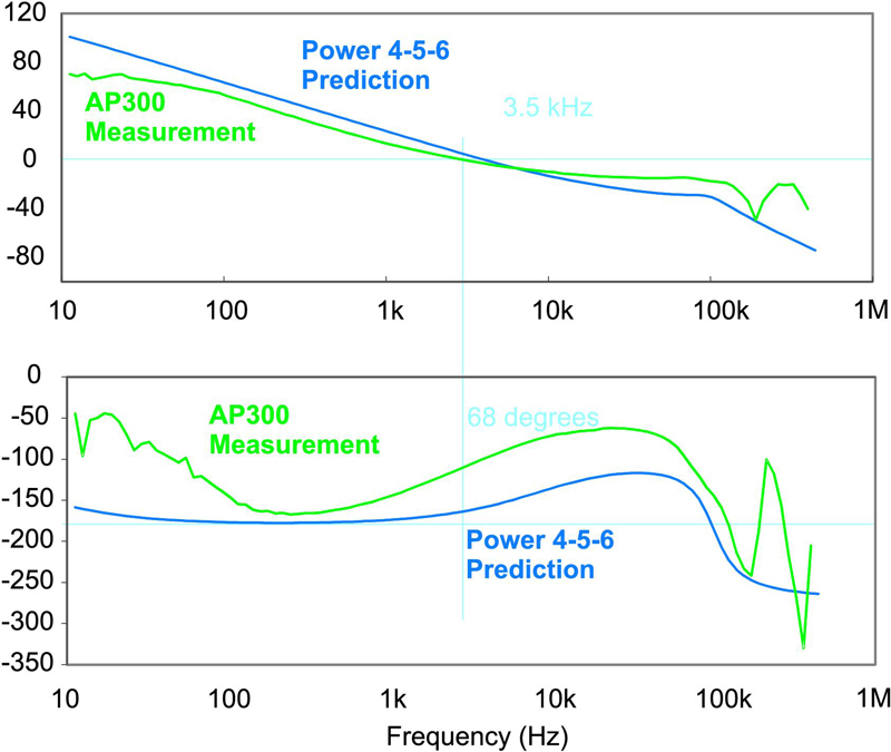
Figure 2 shows the results obtained for the loop gain measurements. It can be seen that there are discrepancies in the measurement and prediction at all frequencies. This is a common result for multiple-output switching power supplies, which is one of the reasons that measurements are crucial for ensuring stability of hardware designs. Rarely are the models accurate enough for coupled-inductor power stages to properly predict stability of the system and ensure a reliable product.
Click image to enlarge
Figure 2: Initial Loop Gain Measurements versus Predicted Results
It is important to understand which factors affect the discrepancies in the loop predictions and measurements. There are two blocks of the system that must be explored – the power stage and the compensation network. Both of these blocks can vary significantly from their theoretical predictions.
Predicted Loop Using Power Stage Measurements
In the last article of this series, the variation in measurements and predictions were discussed for the power stage gain. The curves are repeated below in Figure 3.
Click image to enlarge
Figure 3: Variation in the Power Stage Predictions and Measurement
Variations of the power stage model were due to inaccuracies when the coupled-inductor output is modeled as a single-output converter. Very little has been written on this topic since it is not easily amenable to analysis. To obtain a proper model, an approach similar to Vorpérian’s work on the coupled-inductor Sepic converter would be needed.
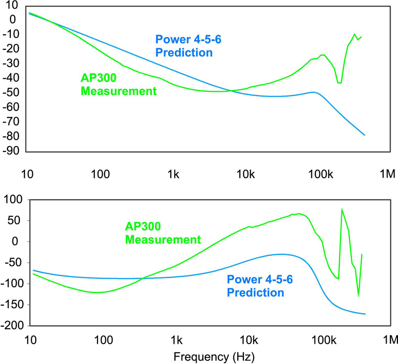
In order to proceed with the controller design, a decision is often made to work with the actual measured power stage rather than the predicted results. The AP300 analyzer system, working with the design software POWER 4-5-6 [2-3], takes the measured results for the power stage, and cascades this with the predicted transfer function of the operational amplifier circuit.
Click image to enlarge
Figure 4: Predicted Loop Gain Using the Measured Power Stage, and Theoretical Compensator. This is Compared to the Measured Loop Gain
Figure 4 shows the measured loop gain versus the combination of the measured power stage and the predicted compensator. It can be seen that the prediction and measurement are now much closer to each other. Variations still persist in the very low-, and very high-frequency regions of the measurement. Since the predictions of this loop gain use the actual measurements of the power stage, these remaining discrepancies suggest that the operational amplifier does not perform according to the predicted model.
The crossover frequency of the loop is at approximately 3.5 kHz, and the measured phase margin was 68 degrees. This was achieved using a very simple Type I compensator.
Limitations of the Operational Amplifier
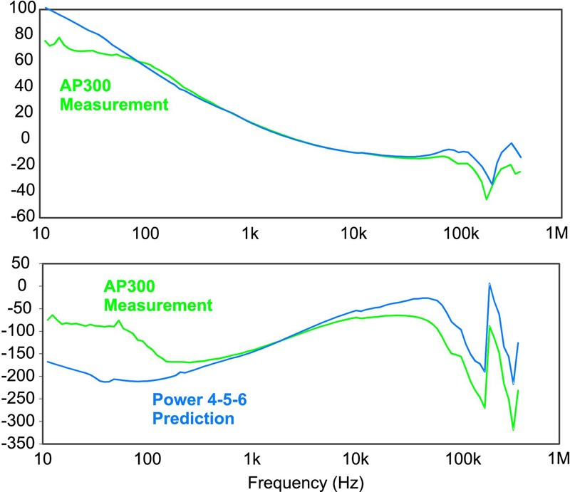
To measure the operational amplifier response, we can still inject a signal with the same circuit shown in Figure 1. The amplifier response is obtained by connecting Channel A of the AP300 Analyzer to the output of the power supply, and Channel B to the output of the error amplifier. The measured and predicted responses are shown in Figure 5.

Click image to enlarge
Figure 5: Measured and Predicted Error Amplifier Compensation
There are two areas of variation in Figure 5. One is at low frequencies, up to 100 Hz, and another is at high frequencies, from 100 kHz. At low frequencies, the open-loop gain limit of the operational amplifier is encountered. This is specified as a worst-case of 65 dB in the datasheets, and measured at around 70 dB. Careful measurement is needed to extract this data, and a large injection signal is required to get clean results. At high frequencies, the gain-bandwidth limitation of the amplifier is encountered. This is often lower than expected due to the high-noise environment in which the amplifier must operate.
There are practical limitations to how much both of these regions can be improved. The gain limitation at low frequencies can be difficult to improve upon due to noise at the amplifier terminals. Although this noise is at a very high frequency, it still carries low-frequency modulated information. It is quite common to require bypass capacitors across all three terminals of the operational amplifier to improve the noise issue.
The gain-bandwidth problem is also hard to overcome. Working with a higher performance amplifier usually exacerbates the noise problems, and makes the converter impossible to control.
Summary
The control loop on the five-output converter was closed using a Type I compensator. This was possible since the complexities of the coupled-inductor power stage model introduce a zero in the measurements that makes a Type II compensator unnecessary.
Reliable design of the feedback loop is done using a combination of the measured power stage, and predicted feedback components. The final measured result is close to predictions, with discrepancies at low and high frequencies caused by the limitations of the error amplifier.
References
1. “Power Supply Design Volume 1: Control”, full color textbook by Dr. Ray Ridley, available at www.ridleyengineering.com/book.htm.

2. POWER 4-5-6 Design and Simulation Software available from www.ridleyengineering.com/software.htm.
3. AP300 Frequency Response Analyzer www.ridleyengineering.com/analyzer.htm