Once limited to simple devices like walking or running step counters, wearable devices have become more advanced seemingly overnight. From vibration-from-speech generating vests for the deaf, to Google Glass, to advanced fitness activity trackers, to night vision equipment, to heads-up imaging displays, wearable devices have become a part of the mainstream consumer, military, and industrial markets.
A “wearable” can be defined as a product that is worn by the user for an extended period of time and in some way, enhances the user’s experience as a result of the product being worn. A “smart” wearable adds connectivity and independent data processing capability to the device. Wearables are divided into five application sub-categories: fitness/wellness (activity monitors, fitness bands, foot pods, and heart rate monitors), infotainment (smart glasses/goggles, smart watches, and imaging devices), military (night vision equipment, heads-up displays, exo-skeletons, and smart clothing), and industrial (body-worn terminals).
These categories have different market forces driving their adoption rates. For the military, it’s the desire to improve situational awareness, maps/routes, combat efficiency, and saving lives. For industrial, the main drivers are improving production line efficiency and tracking capability. For infotainment, it’s the continually exploding gaming market with cutting edge imaging and virtual reality, as well as the increasing number of devices able to connect wirelessly to smart phones to become part of the “internet of things” (IoT). Finally, for the wellness and medical segments, the key driving forces include rising life expectancy, curtailing escalating medical and insurance costs, the desire to prolong a healthy life, and to reduce hospital stays.
Bio-stats for wellness
Bio-stats are vital signs that measure the human body’s basic functions. These include body temperature, pulse/heart rate, respiratory rate and blood pressure. These are critical because an adverse change in vital(s) may indicate a decline in health, and vice-versa. Hospitals and doctor’s offices are obviously well equipped with expensive devices to measure these bio-stats.
Imagine how much more quality-of-life could be improved if these bio-stats could be efficiently and inexpensively measured outside the medical arena. For example, in the home or at work, lifestyle and behavior modifications could be made real time “on-the-fly”, improving health and possibly extending or even saving lives. Fortunately, a combination of device cost reductions and advanced sensor technology has improved to the point where the proliferation of medical and wellness smart wearables is increasing.
These devices include simpler “single vital sign” units that attach to the body, to more sophisticated full-body sensor-filled exo-skeletons. But, from an integrated circuit (IC) electronics standpoint, partitioning and efficiently powering these types of wearables is not trivial.
Typical smart wearable device
What makes typical smart wearable device function? Well, one could think of it as a miniature embedded system. The exact partitioning would obviously depend on the device itself; however, generally speaking the core architecture of a smart wearable is a combination of the following:
• a microprocessor or microcontroller or similar IC
• some sort of micro-electromechanical sensors (MEMS)
• small mechanical actuators
• Global Positioning System (GPS) IC
• Bluetooth/cellular/Wi-Fi connectivity to collect/process and sync data
• imaging electronics, LEDs
• computing resources
• rechargeable or primary cell (non-rechargeable) battery or battery pack
• support electronics.
A wearable unit’s primary design goals are usually to have a compact form factor, low weight for wearability/comfort and possess ultralow energy consumption to extend battery run time/life. However, powering these devices efficiently and accurately with minimal current draw is not so simple.
Some of the key issues associated with powering smart wearables include the following:
1) Low current consumption from the power management IC in a battery-powered device is paramount for increased run time. A micropower or a nanopower conversion IC is necessary.
2) A MEMS sensor requires power from a quiet regulated power source. Busy actuators may also benefit. An LDO or low-ripple switching regulator is ideal for such rails since they have low output noise.
3) Bluetooth/RF/Wi-Fi/cellular connectivity system rails also require low noise. A low dropout regulator or, since output currents can be high, an LDO post-regulated switching regulator or a low-ripple switching regulator are an excellent choice.
4) Processor power (the “brains” of the wearable). From ARM Cortex MCUs, DSPs, GPS chips or FPGAs need a variety of low-voltage rails, spanning a gamut of currents. These can be powered by LDOs or switching regulators.
5) Since not all wearable devices are powered with rechargeable batteries – some may utilize primary cell (non-rechargeable) batteries that need to have long run times between replacements. Therefore, finding a way to estimate battery run time is key.
6) Compact size and low weight makes the wearable device more comfortable for the user. ICs in compact packages provide small solution footprints, thus enabling the device to have both offered in a small form factor and be lightweight.
Ultra-low quiescent current IC solutions
It is clear that an IC solution that solves a wearables application needs, as well as the associated issues already discussed, should have the following attributes:
• Ultra-low quiescent current, both in operating mode and shutdown
• Wide input voltage range to accommodate a variety of power sources
• The ability to efficiently power system rails (some with higher voltages >5V)
• Capability to accurately count coulombs without significantly affecting IC quiescent current (battery consumption) current, to determine battery run time
• Small, light weight and low profile solution footprints
• Advanced packaging for improved thermal performance and space efficiency
For example, recent product introductions from manufacturers like Linear Technology include solutions such as the ultra-low Iq LTC3388/-x buck regulator, the nanopower LTC3331 energy harvesting regulator and LTC3335 buck-boost converter with integrated coulomb counter have most of these attributes already.
The LTC3388 is an ultralow quiescent current synchronous buck converter, which can deliver up to 50mA of continuous output current from a 2.7V to 20V input supply. The LTC3388’s no-load operating current of only 720nA makes it ideal for a wide range of battery-powered and low quiescent power applications such as “keep-alive” supplies and wearables. Its hysteretic synchronous rectification optimizes efficiency over a wide range of load currents.
The device also provides over 90% efficiency for loads ranging from 15 μA to 50mA and only requires 720nA of no load quiescent current in regulation, thereby extending battery life. The combination of a 3mm x 3mm DFN package (or MSOP-10) and only five external components affords a very simple and compact solution footprint for a wide array of low power applications. Figure 1 shows the typical LTC3388 application circuit.
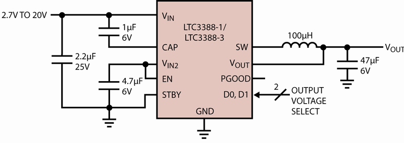
Click image to enlarge
Figure 1. LTC3388-1/-3 Typical Application Circuit
Nanopower quiescent current ICs – LTC3335 and LTC3331
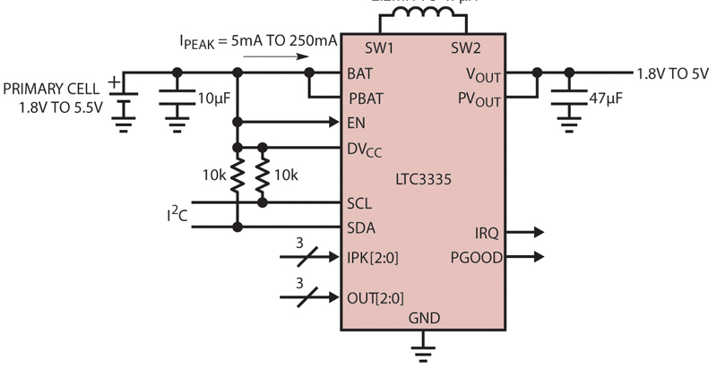
The LTC3335 is a nanopower high efficiency synchronous buck-boost converter with an onboard precision coulomb counter that delivers up to 50mA of continuous output current. With only 680nA of quiescent current and programmable peak input currents from as low as 5mA up to 250mA, the device is ideally suited for a wide variety of low power battery applications, such as those found in wearables and IoT devices. Its 1.8V to 5.5V input range and 8 user-selectable outputs between 1.8V and 5V provide a regulated output supply with an input voltage above, below or equal to the output. In addition, the device’s integrated precision (±5% battery discharge measurement accuracy) coulomb counter provides accurate monitoring of accumulated battery discharge in long-life non-rechargeable battery-powered applications which in many cases have extremely flat battery discharge curves.
Typical applications include wireless sensors, remote monitors, and Linear Technology’s Dust Networks SmartMesh systems. The LTC3335 includes four internal low RDSON MOSFETs and can deliver efficiencies of up to 90%. Other features include a programmable discharge alarm threshold, an I2C interface for accessing coulomb count and device programming, a Power Good output, and 8 selectable peak input currents from 5mA up to 250mA to accommodate a wide range of battery types and sizes. The LTC3335 is available with an operating junction temperature range from -40°C to +125°C in a thermally enhanced, 20-lead 3mm x 4mm QFN package. Figure 2 shows the typical LTC3335 application circuit.
Click image to enlarge
Figure 2. LTC3335 Simplified Application Schematic
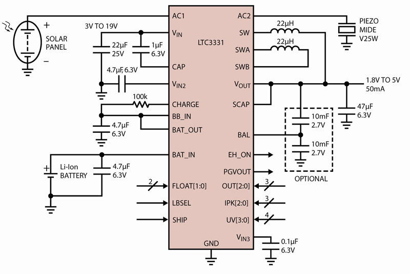
The LTC3331 is a complete energy harvesting solution that delivers up to 50mA of continuous output current to extend battery life when harvestable energy is available. A simple 10mA shunt enables charging of a rechargeable battery with harvested energy while a low battery disconnect function protects the battery from deep discharge. It requires only 200nA of supply current from the battery when providing regulated power to the load from harvested energy and only 950nA operating when powered from the battery under no-load conditions.
The LTC3331 integrates a high voltage energy harvesting power supply, a battery charger, and a synchronous buck-boost DC/DC converter, creating a single continuous regulated output for energy harvesting applications such as those in wireless sensor networks. The energy harvesting power supply, consisting of a full-wave bridge rectifier accommodating AC or DC inputs and a high efficiency buck converter, harvests energy from piezoelectric (AC), solar (DC), or magnetic (AC) sources.
When harvested energy is not available, the rechargeable battery input powers a buck-boost converter that operates over the full battery voltage range up to 4.2V and can regulate whether the input is above, below or equal to the output. The LTC3331 automatically transitions to the battery when the harvesting source is no longer available. The LTC3331’s energy harvesting inputs operate from a voltage range of 3V to 19V AC or DC, making the device ideal for a wide array of piezoelectric, solar, or magnetic energy sources.
Features include input undervoltage lockout threshold settings programmable between 3V and 18V, enabling the application to operate the energy harvesting source at its peak power transfer point. Other features include pin-programmable output voltages and buck-boost peak current limits, a supercapacitor balancer, and an input protective shunt. The LTC3331 is available in a thermally enhanced 5mm x 5mm QFN package. Figure 3 shows the typical LTC3331 application circuit.
Click image to enlarge
Figure 3. LTC3331 Typical Application Circuit
Looking forward
The smart wearables market has exploded in recent years and includes a wide variety of products for the health & fitness, medical, infotainment, military, and industrial application spaces. A new wave of products, including sensor-filled medical health and wellness wearables can monitor key bio-stats such as heart rate and blood pressure outside of a medical facility, resulting in opportunities for more pro-active, healthier lifestyles.
The core architecture for a smart wearable device depends on the product type, but essentially consists of a micro-controller, MEMS sensor(s), wireless connectivity, battery and support electronics. Devices like the ultra-low Iq LTC3388 energy harvesting buck regulator, and for nanopower consumption, the LTC3331 energy harvesting buck regulator & LTC3335 buck-boost regulator with integrated coulomb counter can greatly simplify and improve the performance of smart wearable devices.
 PDF
PDF