Comparing Dead-time Losses for eGaN FETs and Silicon MOSFETs in Synchronous Rectifiers
There have been several comparisons of eGaN FETs with silicon MOSFETs in a variety of applications, including hard-switched, soft-switched, and high-frequency power conversion. These studies have shown that eGaN FETs have large efficiency and power density advantages over silicon MOSFETs. Here we’ll focus on the use of eGaN FETs in synchronous rectifier (SR) applications and the importance of dead-time management. We show that eGaN FETs can dramatically reduce loss due to dead-time in synchronous rectifiers above and beyond the benefits of low RDS(on)and charge.
Early high frequency switch-mode power converters most commonly used a fully controlled switch (S1) and a diode rectifier (S2), in a half-bridge configuration [1]. Figure 1a shows an example of a buck converter with such a configuration. As power MOSFETs became more affordable and higher efficiency more important, designers began to replace the diode with a MOSFET driven with the complement of the control signal to S1 [2], as shown in Figure 1b. The MOSFET replacement for the diode is referred to as a synchronous rectifier (SR). The use of synchronous rectification is especially important where low output voltages and high currents are required, since the junction voltage of the diode can be a large fraction of the output voltage [3]. As the demand for higher efficiency has spread to more applications, the use of SRs has increased dramatically.

Click image to enlarge
Figure 1. Buck converter with diode rectifier (left) and synchronous rectifier (right)
eGaN FETs are particularly well suited for SR operation. With dramatic across the board improvements in nearly all performance-based figures-of-merit (FOMs) compared to silicon FETs, the result is large gains in converter efficiency and power density [4]. However, there has been one area where silicon MOSFETs appeared to beat eGaN FETs, namely that the higher body diode voltage drop of eGaN FETs vs. silicon MOSFETs can lead to increased SR dead-time losses [5]. Although this could be mitigated with careful dead-time management, the use of an external Schottky diode, or both, this could complicate the design. It was suggested that some of this is balanced by the fact that silicon MOSFET body diodes suffer from reverse recovery, but there is surprisingly little data on this aspect of silicon MOSFETs. A better understanding is needed.
Click image to enlarge
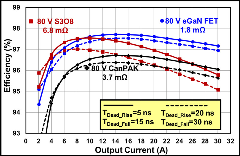
Figure 2. Effect of dead-time on efficiency of 48-12 V, 300 kHz hard-switched buck converters for eGaN FETs and silicon MOSFETs
An experimental comparison of silicon and GaN FETs was done with a set of hard-switched, 300 kHz, 48-12 V buck converters identical in all aspects except the type of FET. Figure 1 shows the results at the minimum dead-time of the gate drive, and with 30 ns additional dead-time (15 ns at each edge). At 30 A output, the additional dead-time causes a 0.22% drop in efficiency for the eGaN FET, and 0.50% and 0.56% for the silicon MOSFETs, more than 2 times worse. The advantage of eGaN FETs is primarily due to their lack of reverse recovery. The remainder of this article will give a detailed explanation of this effect.
Dead-time effects on synchronous rectifier operation
In a practical hard-switched buck converter, both the control FET S1 and the SR FET S2 have non-zero switching times. For very high output currents, large MOSFETs low RDS(on)are required to minimize conduction loss in S2, slowing switching speed due to increased device capacitance. If purely complementary control signals are used for the control FET S1 and the SR S2, the slow MOSFET switching transitions will overlap, resulting in simultaneous conduction of both switches and high losses due to short-circuit shoot-through currents.
This loss is prevented by a delay, or dead-time, in turn-on of the control FET after the SR is turned off td,on, and a corresponding delay in the turn-on of the SR FET after the control FET is turned-off, td,off. During dead-time, the body diode of the SR naturally commutates the inductor current IL. As a result, the switching waveforms for S2 are similar to the case where a diode rectifier is used, as shown in Figure 3, which also shows the negative rectifier current due to reverse recovery and the associated charge QRR, to be discussed later in this article.

Click image to enlarge
Figure 3. Synchronous rectifier waveforms including body diode dead-time conduction and reverse recovery
Dead-time causes additional loss and must be carefully managed if high efficiency is desired. Non-zero dead-time causes loss in two ways: body diode voltage drop and reverse recovery. eGaN FETs have high body diode voltage drop compared to silicon MOSFETs, but they have no reverse recovery [6]. We show that for 80 V FETs reverse recovery loss in silicon MOSFET body diodes can dominate. At lower voltages, which are not the focus of this article, the body diode voltage drop typically dominates losses and eGaN FET dead-time loss can be mitigated by employing a low voltage Schottky diode in parallel with the SR or by dead-time management [5].
Dead-time losses due to reverse voltage drop
During dead-time, the body diode conducts the inductor current IL. Assuming IL is approximately constant and a switching period TS, the dead-time loss due to the body diode voltage drop VS2,diode is simply

In silicon MOSFETs, this body diode comprises the PN junction formed between the drain epitaxial layer and the source wells. This diode has a forward voltage drop VS2,diode of a standard silicon junction diode, i.e. 0.6 - 0.8 V.
The effective body diode in an eGaN FET arises when the gate and source are connected. A negative VDS causes the gate voltage to increase above the drain. Upon reaching the threshold voltage VT, the channel begins to conduct current in the reverse direction, thus emulating diode behavior. The voltage drop is thus slightly larger than the threshold voltage at nominal currents, so that VS2,diode ≈ 2.5 V.
The higher VS2,diode for eGaN FETs means that dead-time conduction losses are substantially larger than those for silicon MOSFETs. This can be mitigated via an external Schottky diode or by dead-time management [5]. The high speed of eGaN FETs means that much smaller dead times can be used than are possible for silicon MOSFETs, but many outdated PWM controllers do not allow the user to access this capability.
However, we show in the next sections that reverse recovery can result in much higher losses than body diode conduction in silicon MOSFETs. These losses can far exceed the body diode conduction losses of eGaN FETs.
Reverse recovery review
Although reverse recovery is a major loss mechanism, it is frequently ignored due to the lack of good data and a challenging analysis [7]. However, it is a major source of switching loss, often dominating all other switching loss mechanisms. When using silicon MOSFETs, reverse recovery losses require attention when high performance is desired.
Reverse recovery is a phenomenon of PN junction diodes. When a diode conducts a current id = IL in the forward direction, a population of minority carriers is injected into the depletion region of the junction. The size of this carrier population corresponds to the magnitude of IL. For various reasons, its size lags changes in id, with a time constant dependent on both transit time and carrier recombination time [8], [9]. eGaN FETs body diodes are majority carrier devices with no PN junction, hence they do not exhibit reverse recovery.
Figure 4 shows typical control switch S1 turn-on waveforms, which start with the body diode of S2 conducting IL during td,on, and end with S1 conducting IL and the diode of S2 fully off. When S1 is turned on, the current iS2 starts decreasing due to S1 carrying an increasing portion of IL. When the control FET current reaches IL, iS2 = 0, and an ideal diode would stop conducting at this point.

Click image to enlarge
Figure 4. Control switch S1 turn-on waveforms showing dead-time and reverse recovery. Current waveform of rectifier S2 show for reference
Since the population of minority carriers lags changes in id, there are still enough carriers in the depletion region of S2 to conduct current. In other words, the diode stays on and a shoot-through current results, otherwise known as the reverse recovery current. This current increases to a maximum of IRRM, at which point the minority carrier population has decreased to the point that it cannot support the current. The current then decays with time constant tRR until the iS2 = 0 and iS1 = IL and the diode is off. The total recovery time is defined as tRR.
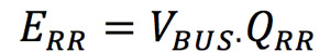
Figure 4 also defines the typical parameters associated with reverse recovery: IRRM, mRR, QRR, tRR, and tRR. IRRM is the peak value of the recovery current, equal to the peak magnitude of the negative rectifier current. The rate of current change during turn-on is mRR, tRRis the recovery time constant, and QRR and tRR are the recovery charge and time, respectively. During reverse recovery, the charge QRR must be supplied from the bus voltage, so the switching loss due to QRR is
Silicon MOSFET data sheets often supply numbers for QRR and tRR under unrealistic conditions, i.e. mRR = 100 A/µs and junction temperature Tj = 25°C. In reality, QRR depends heavily on IL, mRR, Tj, and the amount of time the diode has been conducting before diode turn-off. These dependencies are discussed in [8], [9], but the key interest here is the dependency on forward conduction time td,on.
For a very short dead-time, QRR approaches zero. As td,on increases, the minority charge in the junction builds up to a maximum value that is a function of IL, and both QRR and tRR increase with it. This reduces tRR and IRRM, hence reducing QRR losses in the SR. Once td,on is long enough for the depletion region charge to reach its maximum, further increases in dead-time will not result in additional QRR losses. Changes in td,off should have no effect on reverse recovery losses because the control FET remains off for this part of the cycle, and the shoot-through condition does not exist.
Unfortunately, measurement of reverse recovery parameters is difficult, error-prone, and highly dependent on the test setup, which often doesn’t resemble real-world operation [7]. This fact, combined with a shortage of usable analytic and modeling tools, leads to poor or non-existent accounting for reverse recovery losses. However, there is another way to approach the problem.
If one plots converter loss versus dead-time, we should see two effects in silicon MOSFET SRs. Dead-time losses due to body diode voltage drop should increase linearly in proportion to the total dead-time (td,on + td,off). Dead-time losses due to reverse recovery should be very small for td,on ~0, and as td,on increases, these losses should increase rapidly at first and then at a slower rate proportional to dead-time. Finally, td,off does not affect reverse recovery. eGaN FETs should only show the linear dependence on total dead-time, although the slope should be higher than a silicon MOSFET SR due to the higher VS2,diode.
Measurements
Figure 5 shows three buck converter power stages designed for 48-12 V operation at 300 kHz with 80 V FETs and L = 4.7 μH. These are identical in layout and have been specifically designed for comparison of different power transistors [10]. The center converter uses EPC2021 eGaN FETs, and the other converters use state of the art Si MOSFETs. The values of td,on and td,off were varied, and losses measured.

Click image to enlarge
Figure 5. 48-12 V test converter power stages with 80 V transistors: 3.7 mΩ CanPAKTM Si MOSFET (left), 1.8 mΩ eGaN FET (center) and S308 Si MOSFET (right). Each board has 50 mm sides
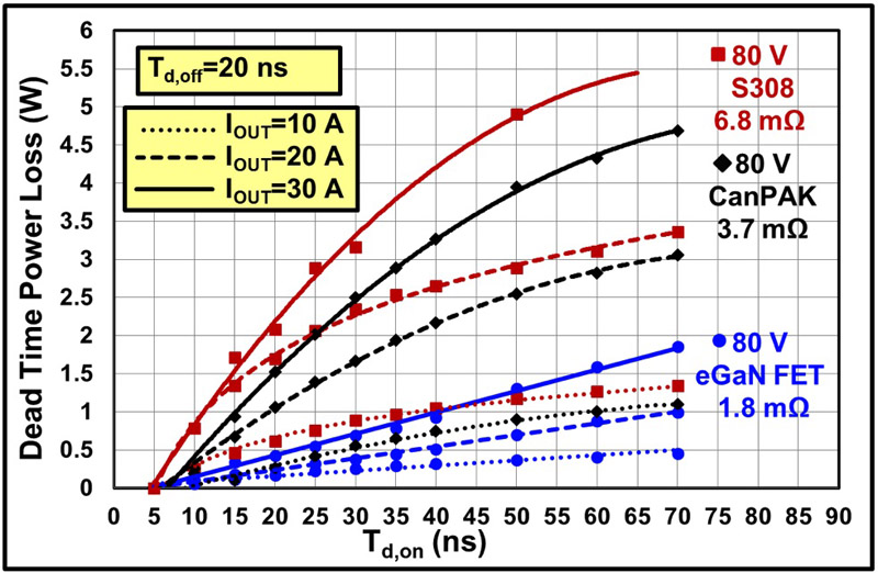
Since this article is concerned with the effects of dead-time, the minimum dead-time case is used as a baseline and subtracted from all loss measurements. This enables quantification of the losses due to dead-time effects. Figure 6 shows these results. As td,on is increased, we see the following: for Si MOSFETs, there is a large initial increase in loss due to QRR, which then approaches an asymptote of constant slope due to VS2,diode, as expected. For the eGaN FET, we see that losses follow a line of constant slope due to VS2,diode for the entire range of td,on, also as predicted.
Click image to enlarge
Figure 6. 48-12 V, 300 kHz test converter dead-time losses for turn-on (top) and turn-off (bottom) for eGaN FETs and selected Si MOSFETs.

Click image to enlarge
Figure 6. 48-12 V, 300 kHz test converter dead-time losses for turn-on (top) and turn-off (bottom) for eGaN FETs and selected Si MOSFETs.
The slope of the eGaN FET loss curve is higher due to the larger voltage drop of the reverse diode conduction. Although the slope is higher, the initial high loss of the Si MOSFETs means that even for large td,on, the reverse recovery loss of the Si MOSFETs far exceeds that due to the reverse voltage drop of the eGaN FETs. As td,off is increased, we see a linear rise in loss due to dead-time, with a higher slope for eGaN FETs, as predicted. The large benefit of eGaN FETs at turn-on far outweighs the small turn-off dead-time benefit of Si MOSFETs.
Expanding potential
The experimental results clearly indicate the large efficiency penalty due to reverse recovery in silicon-based power MOSFETs. Furthermore, while past discussions of dead-time control for eGaN FETs have focused on the need for managing body diode conduction losses through dead-time management or Schottky diodes, it is clear that dead-time management can be far more critical for Si MOSFETs.
This is challenging for Si MOSFETs due to the very large switching figures-of-merit and subsequent slow switching transitions. Hence, for Si MOSFETs, dead-time must be carefully optimized in order to balance QRR losses against shoot-through losses due to switching transition overlap. This problem is exacerbated by the fact that reverse recovery parameters are highly dependent on temperature and load current. Since switching transition overlap is likely to accelerate device failure, most PWM controllers designed for silicon MOSFETs choose long, non-optimum dead times that worsen reverse recovery loss.
The extremely rapid transition speed of eGaN FETs and the freedom from reverse recovery make it possible to use very small dead times, boosting efficiency while maintaining high reliability. As GaN ecosystems continue to grow, it is expected that new controllers will become available that will unlock even more of GaN’s potential.
Efficient Power Conversion (EPC)
References
[1] R. W. Erickson and D. Maksimovic, Fundamentals of Power Electronics, Second. Springer, 2001, p. 912.
[2] R. Blanchard and R. Severns, “MOSFETs move in on low voltage rectification,” in Official Proceedings of the Ninth International PCI, 1984, vol. 84, pp. 29–31.
[3] D. Reusch and J. Glaser, DC-DC Converter Handbook - A Supplement to GaN Transistors for Efficient Power Conversion, 1st ed. Power Conversion Publications, 2015, ISBN 978-0-9966492-0-9.
[4] J. Glaser, J. Strydom, and D. Reusch, “High Power Fully Regulated Eighth-brick DC-DC Converter with GaN FETs,” in PCIM Europe 2015; International Exhibition and Conference for Power Electronics, Intelligent Motion, Renewable Energy and Energy Management; Proceedings of, 2015, pp. 406–413.
[5] J. Strydom and D. Reusch, “eGaN® FET-Silicon Power Shoot Out Volume 12: Optimizing Dead Time,” Power Electronics - Penton Electronics Group, Jan. 2013.
[6] A. Lidow, J. Strydom, M. de Rooij, and D. Reusch, GaN Transistors for Efficient Power Conversion, 2nd ed. Wiley, 2014, ISBN 978-1-118-84476-2.
[7] C. Mößlacher and O. Guillemant, “Improving Efficiency of Synchronous Rectification by Analysis of the MOSFET Power Loss Mechanism,” Infineon Technologies, Mar. 2012.
[8] X. Kang, A. Caiafa, E. Santi, J. L. Hudgins, and P. R. Palmer, “Parameter extraction for a power diode circuit simulator model including temperature dependent effects,” IEEE Applied Power Electronics Conference and Exposition (APEC), March 2002, Vol. 1, pp. 452–458.
[9] P. O. Lauritzen and C. L. Ma, “A simple diode model with reverse recovery, ”Power Electronics, IEEE Transactions on, vol. 6, no. 2, pp. 188–191, Apr. 1991.
[10] D. Reusch, J. Strydom, and A. Lidow, “Thermal Evaluation of Chip–Scale Packaged Gallium Nitride Transistors,” IEEE Applied Power Electronics Conference and Exposition (APEC), March 2016, pp. 587–594.


