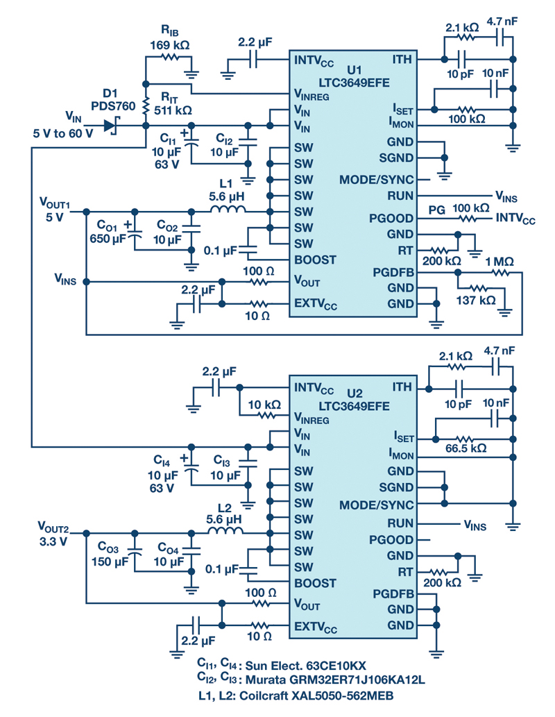
Figure 1. The 5 V output converter (U1) provides hold-up power for protected load on the 3.3 V output (U2). Note that the pin MODE/SYNC of U1 is left floating, allowing the LTC3649 to enter boost mode
The LTC3649 is a monolithic step-down regulator capable of operating from an input voltage range of 3.1 V to 60 V, and efficiently producing a single resistor-programmable output voltage at up to 4 A of output current. These features alone make it a compelling industrial or automotive supply for output voltages from (VIN– 0.5 V) to ground. One unique feature of the LTC3649 is that it is capable of providing power to critical systems when there is a power outage, without any extra components.
Hold-up circuits supply power to critical systems when the main power rail fails, allowing them to perform important housekeeping tasks, such as data retention, for a short period before all available energy is lost. Typical hold-up solutions employ dedicated controllers and large storage capacitors,1, 2such as with LTC3310 and LTC3643. Thus, additional costsand complexities are warranted if the critical circuits require significantpower and hold-up time. But if the required hold-up energy is relatively low, the LTC3649 can easily perform this task with no additional circuitry.
The dual output converter described herein works as a conventional step-down power supply under normal operating conditions, but during a power interruption, the converter itself becomes the energy source, maintaining the programmed output voltage to critical circuits. To perform this task, U1 becomes a step-up converter when input voltage is disconnected, which causes U1 to discharge its output capacitor in order to providehold-up energy.
Dual Output Converter and Hold-Up Circuit
Figure 1 shows a hold-up design using the LTC3649. Under normal conditions, the unregulated rail, VIN(VINSvia a blocking diode) supplies a converter based on U1 (Converter A). This converter works in buck mode, generating a stable 5 V on VOUT1. VINSis connected to a U2-based second converter (Converter B), which supplies 3.3 V on VOUT2to a critical load. When VINfails, Converter A enters boost mode and maintains its programmed output voltage (VINS) by discharging its output filter capacitors C01and C02. Resistors RITand RIBprogram this voltage level. The PGOOD (PG) signal produced by U1 can be used to communicate the power failure to systems that can disconnect noncritical circuitry to preserve energy. The MODE/SYNC pin is left floating to allow the LTC3649 to enter boost mode.
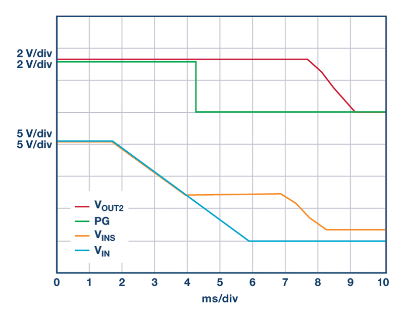
Figure 2 shows what happens to the LTC3649 in a boost mode. For the first 7 ms of the capture, all voltages are stable. At 7 ms, the power is turned off; both VINand VINSbegin to decline. When VINSreaches 8 V, it stabilizes and the PG signal changes state, signaling the beginning of the VOUT1collapsing. VINSremains at 8 V as long as C01and C02have charge. VOUT2holds constant during the entire process, supplying steady power to the critical load long after the power is interrupted. Analog Devices has created an LTspice model.
Click image to enlarge
Figure 2. When the input voltage VIN drops, the converter U1 boosts VOUT1 to maintain VINS at 8 V. VINS provides power to keep VOUT2 in regulation for over 20 ms after VIN drops out
Conclusion
LTC3649 is a monolithic step-down regulator with integrated power MOSFETs. It is highly efficient, with low quiescent current, which is importantin many battery-operated systems. It is also highly versatile, with programmable frequency, a wide VINrange up to 60 V, and an output voltagerange down to ground. It simplifies the design of automotive and industrialsupplies, especially when its inherent ability as a hold-up circuit is taken into account.