A Deep Dive into High-Efficient LED Drivers for Low-Profile Display Applications

LED panel displays can be the main source of laptop battery drain – accounting for 50-60% of the system loading
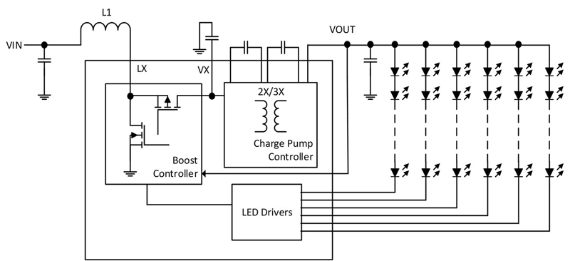
Figure 1: Conventional LED boost architecture simplified circuit diagram
Laptop battery drain has a significant impact on the battery run-time of the laptop system. In this article, we explore the efficiency and performance of the LED driver and introduce a novel, 2-stage architecture that consists of a synchronous boost followed by a charge pump multiplier. We compare the 2-stage architecture to the performance of a traditional single stage boost architecture and conclude that it provides significantly improved efficiency with a smaller and thinner output inductor, which is ideal for use in low-profile display applications. The second part of this article studies screen display-dimming techniques and concludes that analog dimming or DC modulation can further enhance efficiency. The combined impact of the 2-stage architecture with analog dimming provides significant efficiency improvements and extends system battery run time.
Typical LED boost architecture
Typically, power architects use conventional, single-stage asynchronous boost architecture to convert the low input voltage from the battery cells to the higher voltage, display driver LED strings. Due to the high output voltage requirement, architects often favor an external Schottky diode over a high-voltage, integrated P-channel field-effect transistor (FET). The high-voltage FET can be large and consume valuable controller IC real estate, while the external Schottky tends to reduce control complexity at a relatively low cost. However, the external Schottky typically reduces efficiency by 0.5% to 1%. Figure 1 shows a simplified circuit diagram for the conventional LED boost driver.
The control and driver logic for the asynchronous LED boost architecture is relatively simple to implement and use but it has the following disadvantages:
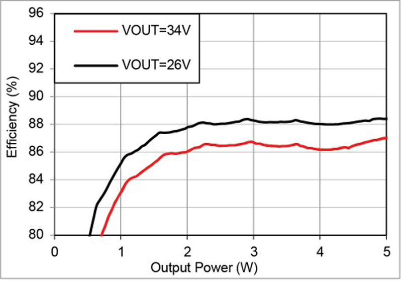
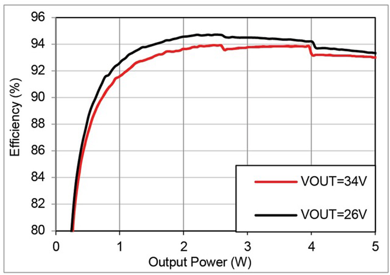
· Efficiency is reduced as output voltage (VOUT) increases due to the increase in the conversion ratio. This can force applications to use fewer series LEDs to reduce the output voltage but also increases the number of parallel LED strings. More parallel LED strings require a wider bezel to accommodate more routing. This conventional architecture also reduces system efficiency due to more losses in the LED current sinks’ regulation voltage (VREG). For a typical VREG of 0.4V and VOUT of 24V, the VREG contributes to a 1.67% system efficiency loss(VREG loss = VREG/VOUT × 100%). Figure 2shows the efficiency impact at two different VOUT levels.
Click image to enlarge
Figure 2: Efficiency drops ~2% as VOUT increases from 26V to 34V at the 5W output power level (VIN = 7.6V)
· An asynchronous architecture creates a path between the input voltage (VIN) and GND if VOUT is shorted to GND, increasing the potential for catastrophic failure. Preventive solutions include either placing an input disconnect FET (such as Q1 in Figure 1) or placing a fuse in the VIN path. This solution requires additional board space and increases the material cost and system efficiency loss.
· In a conventional boost architecture, a larger inductor must be used to attain the highest efficiency. This architecture occupies more board space and increases costs. Critically, it is not possible to create high-efficiency solutions for low-profile applications (<1 mm), such as LED panel displays.
In today’s laptops, the major battery power consumer is the panel display. Improvements in semiconductor processes and application processor management of the system now mean that the display panel is the main drain on battery power, typically consuming 50-60% of the battery power and reducing the system battery run time.
Novel 2-stage LED boost architecture
pSemi and Murata specialize in novel, 2-stage architectures: a 2-stage buck for stepping-down the voltage or a 2-stage boost for stepping-up the voltage. In the LED panel application, a 2-stage boost is used. The first stage conversion is a synchronous buck converter inductive-based boost DC-DC converter. The second stage consists of a capacitive-based charge pump multiplier. The charge pump circuit provides a fixed x2 conversion from the output of the first stage boost to the LED VOUT. The second stage charge pump multiplier is capable of ultra-high efficiency of around 99%, regardless of the input or output voltage.
The fundamental dventage of the 2-stage architecture is that the switching capacitor stage performs most of the power conversion. Capacitors are much more efficient as an energy storage element than an inductor. If the energy can be harnessed correctly, then capacitive energy transfer provides improved efficiency in a smaller area. The first boost converter is now only required to convert to an intermediate voltage level. Therefore, it becomes easier to integrate the lower voltage, synchronous FET. Additionally, the inductor becomes smaller and has a lower profile, ideal for thin panel solutions.
Figure 3 shows how the first stage synchronous boost, the second stage charge pump capacitor multiplier, and the LED drivers are all combined in one monolithic IC.
Click image to enlarge
Figure 3: Integrated LED driver schematic
Combining the 2-stage converter with the LED driver stage provides the following advantages:
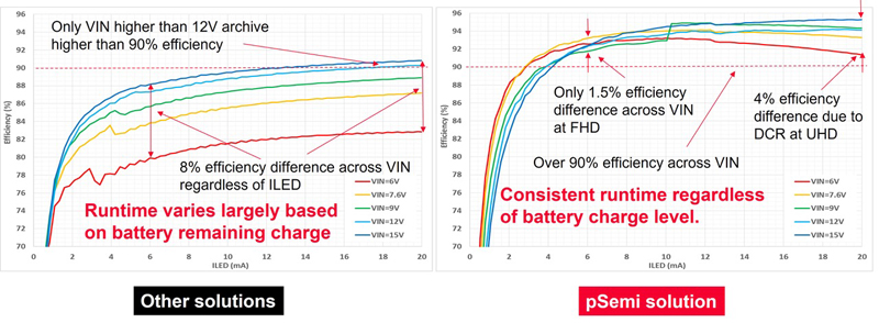
· The combination of the highly efficient charge pump circuit and the boost stage provide higher efficiency compared to the conventional single-stage, LED boost architecture. The output voltage range of the first stage boost is reduced compared to a single-stage boost. So, if VOUT increases, there is no significant impact on efficiency. Additionally, efficiency is more consistent across VIN compared to a conventional LED boost, making the run time much more consistent as the battery depletes. Figure 4 shows the efficiency as VOUT increases, and Figure 5 compares the VIN efficiency between Murata’s and a competitive solution.
· Reducing the output voltage on the boost circuit allows the use of a small, low-cost chip inductor, due to the duty cycle decrease. The small chip inductor has a maximum 20V rating to avoid inductor internal leakage or shoot-through current, making it unsuitable for conventional LED boost for high VOUT applications.
Click image to enlarge
Figure 4: Efficiency drop of <0.5% as VOUT increases from 26V to 34V at the 5W output power level VIN = 7.6V
Click image to enlarge
Figure 5: Consistent efficiency across VIN compared to competitor solutions
· The lower boost output voltage allows the use of a synchronous conversion, eliminating the need for an external diode. This results in a more highly integrated solution with improved efficiency.
· Each FET in the charge pump and boost circuits only experience a small voltage step across drain to source. This multiple-step architecture allows the use of much lower-voltage FETs, which reduces on-time and switching losses.
· The EMI signature is improved through the following: the voltage change across the inductor is lower when compared to the single-stage converter, and the architecture uses a soft-charging charge pump that reduces noise compared to traditional single-stage architecture.
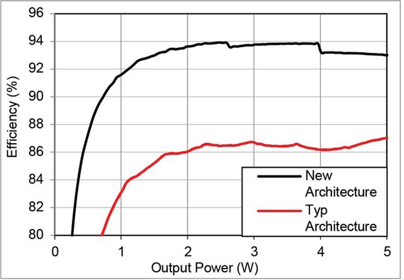
Figure 6 shows the efficiency comparison between the unique two-stage boost architecture and the conventional single-stage boost architecture.
VOUT for both devices is 34V, and both devices use a 4.7 µH inductor. However, the inductor used by the unique LED boost architecture is a chip inductor (DFE322512F-4R7M) in a compact 3.2 × 2.5 × 1.2 mm case size. The conventional LED boost architecture uses a large wire-wound inductor (SPM5020T-4R7M) in a 5.4 × 5.1 × 2.0 mm case size.
Click image to enlarge
Figure 6: Efficiency comparison between unique and conventional LED boost architectures
Improving system efficiency through LED driver performance
Using the 2-stage architecture LED boost provides significant efficiency improvement for the LED backlight in LCD panels. Besides the new architecture, using analog dimming for LED dimming can further improve system efficiency compared to digital PWM (DPWM) dimming. This section describes this in detail.
The two established methods to adjust LED brightness include analog dimming and DPWM dimming, which can also be referred to as DC modulation (analog dimming) and PWM modulation (DPWM dimming).
Table 1 lists the key operating comparisons between the two modulations. Analog dimming has more benefits over DPWM, but the LED color temperature issue causes many display engineers to avoid using DC modulation. But with the advancement in LED technology, the LED color becomes more consistent across the LED current, so color temperature is no longer a critical concern.

Click image to enlarge
Table 1. Analog dimming vs DPWM dimming operating comparison
These benefits show how analog dimming offers higher system efficiency compared to PWM modulation.
Conclusions
We can conclude that a traditional single-stage, asynchronous—or even synchronous—boost LED driver results in relatively low efficiency when compared to the novel 2-stage architecture. The 2-stage design, based on a synchronous boost followed by charge pump multiplier, improves system efficiency. It facilitates the use of low-profile, low-cost chip technology output inductors, which are ideal for low-profile LED panel designs. In general, the display panel is a major source of battery power drain, estimated to be 50%-60% of the system loading. The efficiency improvement of the 2-stage architecture can significantly extend the battery run time in a laptop system.
The article compares different approaches to display dimming and concludes that analog dimming or DC modulation is the most effective method. This technique can be applied with the 2-stage architecture to provide further efficiency improvements and increased battery run-time.
 Single.jpeg)