A High-Performing Solution is an End-Product of Right Choices - USB-PD Solutions: Part 4 of 4

A 100 W 94 % efficiency USB-PD solution
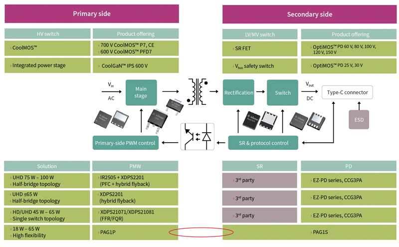
Avoid complexity, incompatibility and shorten time-to-market! Infineon with its broad portfolio of high-performing and high-quality USB-PD solutions help engineers break through the barriers in fast charging designs at a competitive cost.
The ever-increasing battery capacity and need for shorter charging time are pushing the power requirement for chargers to higher levels. It will be a challenge to put a large power supply design into a small form factor case. A number of innovations have been already considered, such as zero voltage switching (ZVS) topology, high-performance power switches, innovative packages or even the use of wide-band-gap materials to meet today’s design requirements. This article introduces a 100 W USB-PD solution, and will also explain how to employ power switches and a new topology to achieve 94 percent efficiency and 2.3 W/in3 power density.
Why selecting the right topology is key to performance?
To obtain excellent power density, a combination of the right topology, dimensioning, and advanced control techniques are required. Looking at the high power mobile charger market, there are several solutions for high power USB-PD chargers, such as PFC + QR and PFC + LLC. However, some drawbacks limit the wider usage of these: the QR cannot achieve soft switching, and it’s difficult to use LLC topology for variable output voltage designs.
Aware of this situation, Infineon has introduced a new topology named hybrid flyback based on an asymmetric half-bridge control (as shown in Figure 1). The half-bridge is driving a conventional flyback transformer in conjunction with a serial capacitor. The main inductance of the flyback transformer and the serial capacitor form a resonant tank, which is used to realize a ZVS behavior of the half-bridge power switches and also provides resonant power transmission during the conventional demagnetization phase of the flyback transformer. During normal operation, the charging cycle and related power are controlled by direct peak current control, while the demagnetization phase is controlled by timing to ensure proper negative premagnetization, which is required for a ZVS condition of the half-bridge power switches.
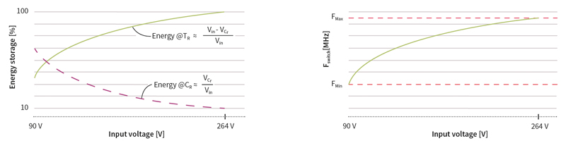
The power circuit in the primary is realized by an LC tank, which is driven by a half-bridge similar to an LLC converter. The resonant inductor Lr represents the series inductance, Lr being either the transformer leakage inductance or the leakage inductance plus an external inductor, and Lm represents the transformer main inductance. The same converter can also be realized by connecting the resonant capacitor Cr and the primary coil of the transformer between the positive node and the midpoint of the half-bridge. When the high-side switch HS is turned on, energy will be stored in Cr and Lm, and the respective stored energy will vary with the input voltage and switching frequency (as shown in Figure 2).
Click image to enlarge
Figure 2 Energy storage distribution and frequency variation diagrams
When the high-side switch HS is turned off, the current in the transformer will force the half-bridge midpoint VHB to drop until the body diode of the low-side switch clamps the voltage. Then, the low-side switch will be turned on at zero voltage, and at the same time, the transformer phase reverses and energy is transferred to the secondary side. When the low-side switch is turned off, the negative current induced in the transformer in the previous phase will force the half-bridge midpoint VHB to increase its voltage until it is clamped by the body diode of the high-side switch HS, similar to the previous phase. HS is switched on under the ZVS condition and LS is switched off, but the current in the transformer resonant tank is still negative, which means that the excess energy in the tank will be sent back to the input.
Why hybrid flyback is the topology of choice?
Compared with other flyback topologies, hybrid flyback transformers need to store less energy, thus helping to reduce the size of the charger.
Hybrid flyback can achieve full ZVS operation on the primary side and full ZCS operation on the secondary side, and the leakage energy is recycled, thereby achieving high efficiency.
The output voltage will change with the duty cycle (as shown in the below formula). For hybrid flyback, it’s much easier to achieve a wide voltage range output, which overcomes the limitations of LLC topology in wide voltage output applications:

Vout: output voltage
D: duty cycle
Vin: input voltage
Lm: transformer inductance
N: transformer turn ratio
Lr: transformer leakage inductance
Real-life example: the 100 W USB-PD reference design from Infineon
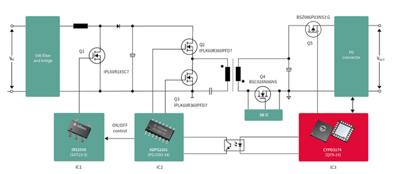
The full solution is shown in Figure 3. The PFC stage utilizes critical-conduction mode IRS2505 and ThinPAK packaged IPL60R185C7 CoolMOS™, and the DC-DC stage uses the digital PWM controller XDPS2201 (the product is coming soon) and IPLK60R360PFD7, while BSC028N06NS used as a synchronous rectification switch, the protocol controller is CYPD3174, and p-channel MOS BSZ086N03NS3 used as an output safety switch.
Click image to enlarge
Figure 3 The 100 W USB-PD solution block diagram
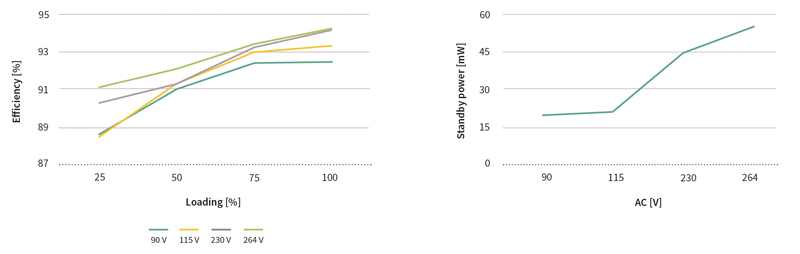
With this setup, efficiency can peak at 94 percent and the standby power is lower than 60 mW.
Click image to enlarge
Figure 4 Efficiency and standby power curve
Highest efficiency: selecting the right high-voltage MOSFET is important
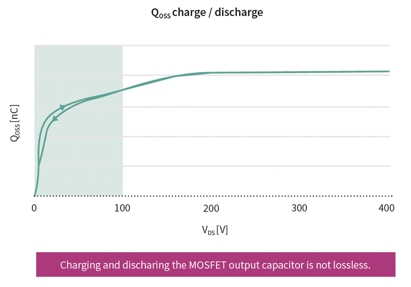
Soft-switching techniques enable devices to operate in ZVS, which means that the MOSFET is turned on only after its drain-source voltage reaches 0 V (or a value close to 0 V). This strategy eliminates the turn-on loss of the device, which is typically the major contributor to the overall switching loss. Unfortunately, all high-voltage SJ MOSFETs suffer from another type of loss due to their “non-lossless” behavior of the output capacitance. This means that when the MOSFET output capacitance (Coss) is charged and subsequently discharged, some energy will be lost. Therefore, even when operating under ZVS conditions, all the energy stored in the output capacitance (Eoss) will not be recovered. This phenomenon is related to the hysteretic behavior of the Coss, as shown in Figure 5, which can be observed performing a Coss charge/discharge cycle with a large signal measurement. This is why these losses are commonly known as Coss hysteresis losses (Eoss,hys).
Click image to enlarge
Figure 5 The Qoss charge/discharge cycle of a SJ MOSFET
Thanks to the latest advancements in Infineon’s state-of-the-art SJ technology, the CoolMOS™ PFD7 series has lower hysteresis losses than previous generations, helping to further improve efficiency.
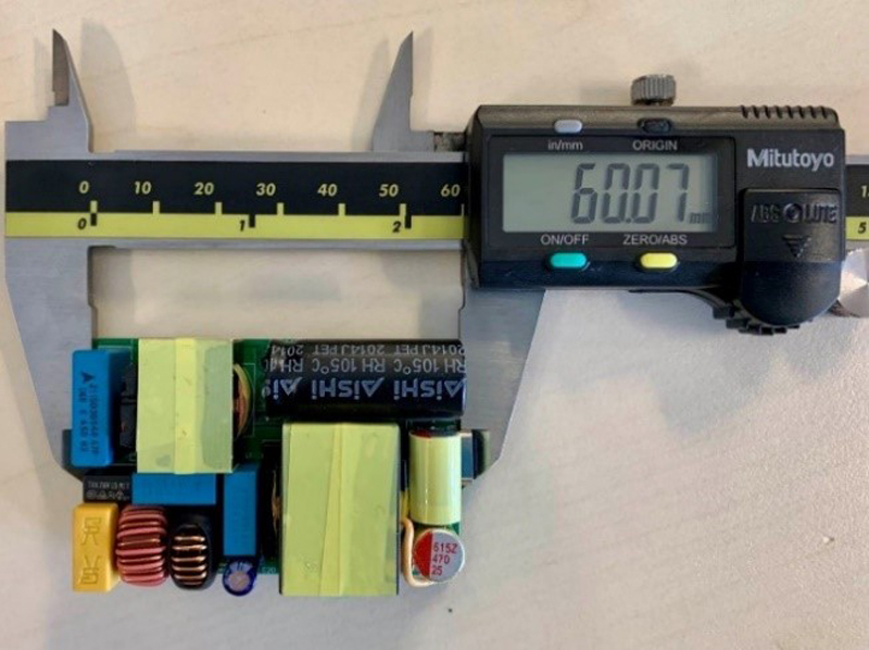
The ZVS hybrid flyback based on the digital XDPS2201 can realize ZVS and ZCS under all input voltage and output current conditions.In addition, it recycles the energy of the transformer leakage inductance. High-performance power MOSFETs can further contribute to achieving 94 percent efficiency for the 100 W USB-PD design in a small, 60 mm x 40 mm 18 mm form factor.
Click image to enlarge
Figure 6 The 100 W 94% efficiency USB-PD reference design in a small form factor from Infineon
Discover our reference designs, boards and design support documents at www.infineon.com/usb-pd!