A New Generation of GaN Devices to Meet AI Server Power Demands
Data center power demand continues to rise, fueled by new massive AI workloads, challenging designers to stringent efficiency targets within the established CRPS form-factor
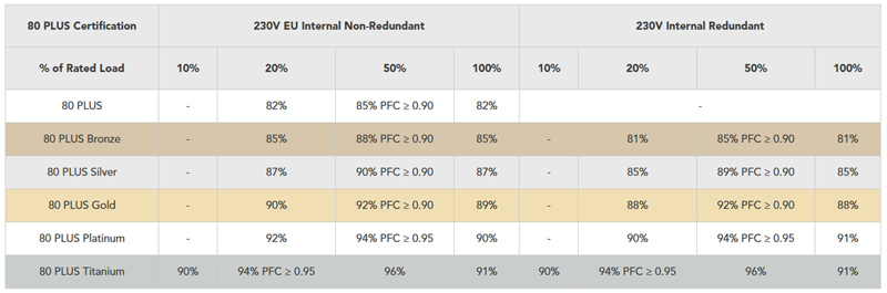
Table 1: 80 PLUS efficiency specifications at 230V input
The rapid development and deployment of massive artificial intelligence (AI) in the cloud - including OpenAI’s ChatGPT, Microsoft’s Bing with AI, plus Google’s Bard and Deep Mind Gemini - is drawing new and more powerful, purpose-designed AI processors into data center servers. Next-generation hyperscale systems are expected to incorporate superchip platforms such as Nvidia’s DGX GH200 ‘Grace Hopper’, which consumes up to 1,600 W per device. The trend is set to increase the typical server power demand from 30-40 kW today to 100 kW per cabinet in the future.
Meanwhile, with the global focus on energy conservation and emission reduction, ambitious ecodesign regulations continue to raise power-supply efficiency targets. The latest European regulations expect server power supplies to exceed the 80 PLUS ‘Titanium’ efficiency specification. Titanium is currently the highest standard in the 80 PLUS certification program, calling for the highest efficiency values across the load range and introducing a new test at 10% to measure light-load efficiency, as described in the table. 80 PLUS Titanium also specifies the power factor should be at least 0.95 at lower load levels, which requires active power-factor correction (PFC).
On the other hand, server rack-size constraints are established and essentially immovable. The demands of the enterprise and hyperscale markets are known to be tough and have driven the Open Compute Project - including Facebook, Intel, Google, Microsoft, and Dell – to define the Common Redundant Power Supply (CRPS) specification. Designed to ensure modularity for easy replacement and maintenance, and flexibility to address different applications and environments, as well as redundancy, CRPS mandates that rack power be provided in a 1U (40 mm) x 73.5 x 185 mm form factor.
As server power demand is set to increase 2x-3x, designers now face an even tougher challenge to satisfy the demands for greater power delivery and significantly higher efficiency within the CRPS form factor. A closer look at a typical compliant power supply provides some insights.
Power Supply Design and Evolution
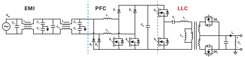
The most used topology for CRPS is a boost PFC stage followed by an LLC resonant converter (figure 1). The first stage performs power-factor correction while transferring the AC utility power to a constant 380 V DC bus voltage. The second stage regulates the voltage and provides isolation, converting the 380 V bus voltage to a 12 V low-voltage output for the subsequent stages. The boost PFC operates at a switching frequency of approximately 65 kHz to achieve optimal efficiency and EMI performance. Switching losses tend to be lower in the LLC resonant converter, such that the frequency is typically between 100 -150 kHz.
Click image to enlarge
Figure 1: CRPS two-stage topology
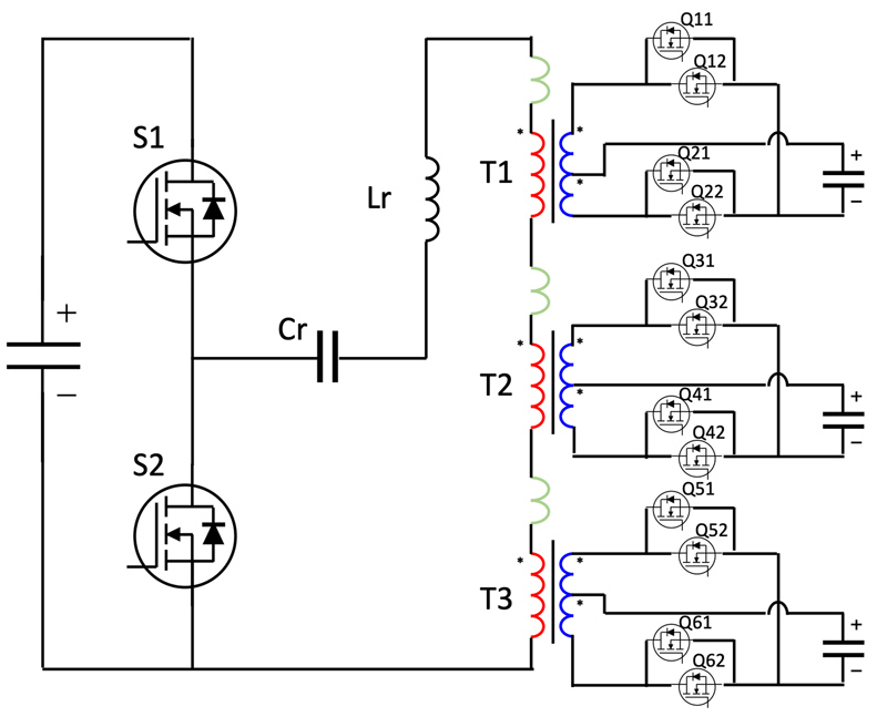
The increasing power demands coming with the era of massive AI workloads call for the CRPS LLC converter to deliver at least 1.5 kW. This is likely to rise further in the future. To deliver 1.5 kW at 12V necessitates a current output of 125 A. This calls for multiple outputs when using LLC transformers, to minimize the conduction loss of secondary windings and synchronous rectifiers (SRs).
Figure 2 illustrates a popular configuration, built with 40V synchronous rectifier (SR) MOSFETs. This circuit combines two SRs in parallel to increase system power density.
Click image to enlarge
Figure 2: Half-bridge LLC converter with three sets of synchronous rectifiers
Traditionally, engineers have combined windings and SRs in parallel to achieve lower winding resistance. However, this approach incurs termination losses that become more pronounced as the switching frequency increases, leading to a decline in overall system efficiency.
Using multiple transformers connected in parallel, instead of windings and SRs, reduces AC-related conduction loss and minimizes leakage flux, resulting in reduced leakage inductance. This approach also simplifies the terminal design and enhances interleaving between primary and secondary windings, especially at terminations where windings connect to SRs.
However, using multiple transformers introduces larger core losses and a larger magnetic size. Matrix transformers can mitigate these losses by ensuring flux cancellation between cores. A matrix transformer combines individual transformers such that primary side windings are connected in series/parallel while secondary side windings are connected in parallel/series. A configuration having primary-side series with secondary-side parallel connection is suitable for the CRPS LLC step-down application.
For a nominal bus voltage of 380 V and 12 V output, as specified by CRPS, the ideal transformer turns ratio is calculated to be 16(𝑁= 𝑉𝑖𝑛 / 2𝑉𝑜). As the design comprises three transformers, a practicable ratio is 15. Hence, in this setup, using primary windings in series and secondary windings in parallel, each transformer requires a ratio of five.
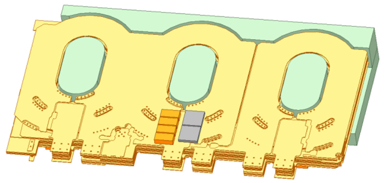
The physical size of the converter remains a challenge, if built using traditional wire-based transformers. PCB-based planar transformers (figure 3) offer a space-saving alternative and are produced using automated processes that can be cost-effective and repeatable for large-scale manufacturing. However, due to the restrictions of PCB windings, planar transformers can only be achieved when the switching frequency is sufficiently high to substantially decrease the number of turns.
Click image to enlarge
Figure 3: Planar matrix transformers for 3-output CRPS LLC module
Raising Frequency with GaN
Replacing silicon MOSFETs with GaN technology allows much higher switching frequency, suitable for planar transformers, while keeping switching losses to enable 80 PLUS Titanium efficiency. GaN transistors also benefit from low conduction losses, due to their low channel resistance when turned on as well as the absence of the intrinsic body diode present in silicon MOSFETs.
However, enhancement-mode (normally-off) GaN HEMTs (high electron-mobility transistors) have a relatively fragile gate. Where MOSFETs can typically handle gate voltage from -10 V to 20 V, with a threshold of 2 V - 5 V, eMode GaN HEMTs have a gate voltage range of -10 V to 7 V. The GaN threshold voltage is typically in the range 1 V to 2 V.
GaN HEMTs thus require precise gate control. However, when using discrete GaN HEMTs in high-power bridge circuits, negative spikes in the gate-source voltage (VGS) at low-side turn-off can exceed the device’s specified maximum. Also, the combined effects of gate-loop inductance and high di/dt can cause severe high-side and low-side VGS ringing. In addition, there is a high risk of shoot-through currents.
Integrating an optimized gate driver in the same package as the GaN HEMT helps designers properly control VGS to avoid these risks. Navitas’ GaNSafe™ devices integrate the GaN HEMT and optimized gate-drive circuitry, adding advanced algorithms for dead-time control and extra safety features needed for applications in the 1,000 W to 22,000 W range. They enable a "digital in, power out" design approach with fast switching, high efficiency, and superior power density. They are conceived to meet the needs of AI-based data centers as well as EV, solar, and energy storage systems.
The devices have zero gate-source loop inductance, which enables switching at up to 2 MHz to maximize application power density. High-speed short-circuit protection is built-in, with autonomous ‘detect and protect’ that acts within 50 ns. Electrostatic discharge (ESD) protection, typically not provided with discrete GaN transistors, is built-in and protects against events up to 2 kV. In addition, with 650 V continuous and 800 V transient voltage capability, they can survive extraordinary application conditions. Programmable turn-on and turn-off speed simplifies meeting EMI regulatory requirements. The devices have extremely low quiescent current and are housed in a 4-pin TOLL package, whereas comparable multi-chip modules can require up to three times as many connections and have poorer cooling capability.
Navitas’ system design center has created power supply reference designs leveraging GaNSafe technology, including two CRPS converters that satisfy 80 PLUS Titanium. These include a 1.5 kW CRPS-ready LLC resonant converter module that uses a 10-layer interleaved planar transformer to fit in a 1U-high 90 x 30.5 x 11 mm form-factor. With GaNSafe devices switching at over 600 kHz, the module’s efficiency exceeds 97.5%. When paired with a 98.5% totem-pole PFC, peak efficiency is over 96% at 50% of full load.
The second design, a 3.2kW CRPS185 data center power platform in the 40 x 73.5 x 185 mm form-factor, reaches over 96.5% efficiency at 30% load, and over 96% from 20% to 60% load. The power density of 5.9 W/cc, equivalent to almost 100 W/in3, represents a 40% size reduction over a comparable legacy silicon approach.
Conclusion
Fulfilling the power demands of massive AI workloads, complying with the established CRPS form factor, and meeting 80 PLUS Titanium efficiency is extremely difficult within the constraints imposed by existing silicon devices. GaN technology allows the high switching frequencies needed to build efficient, high-power CRPS converters and. With gate-drive, system safety, and protection features built-in, these devices ensure reliability and failure resistance meeting the needs of data-center operators.