A New Variation of the Classic Instrumentation Amplifier
While instrumentation amplifiers (IAs) are useful when interfacing to a transducer, there are constraints that hamper the design of variable gain IAs or PGIAs.
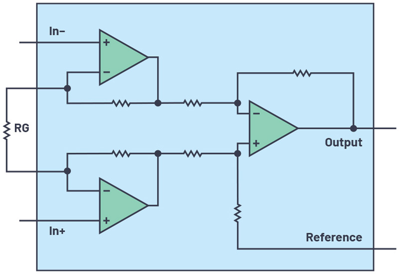
Figure 1. Classic instrumentation amplifier
The need for PGIAs arises because of the often-encountered case of adapting the circuit to a wide range of sensors or environmental conditions.With a fixed gain, suboptimal SNR could compromise precision. Techniques useful in creating accurate, stable PGIAs are discussed in, “Programmable Gain Instrumentation Amplifiers: Finding One that Works for You,” which also points out possible pitfalls.
This article presents another methodology and the design steps to quickly home-in on the external component values needed to create a precise PGIA.
A New Instrumentation Amplifier Architecture
One common instrumentation amplifier architecture is shown in Figure 1.
The gain is set by the external resistor RG. To create a PGIA with such a device, one needs to switch the value of RG, commonly doneusing an analog switch or a mux. However, non-ideal behaviors of analog switches – like switch on-resistance, channel capacitance, and variation of channel resistance with applied voltage – complicate this task.
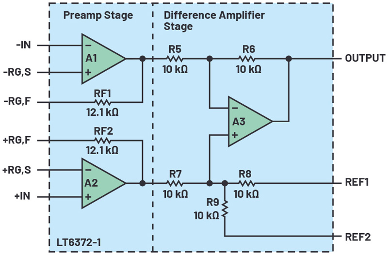
Figure 2 shows a variation on the standard amplifier architecture. The RG pins are broken up as ±RG,S and ±RG,F and individually pinned out and accessible from the device package.
Click image to enlarge
Figure 2. An amplifier architecture like the LT6372-1 allows access to some internal nodes
An important feature of this architecture is the amplifier can switch between distinct gain values while minimizing any gain error because of finite switch resistances.This feature can be used to createa PGIA.
Any resistor programmable in-amp can vary its gain by switching the value of the gain-setting resistor accordingly, but with drawbacks:
- Large gain error due to switch on-resistance (RON) nominal value and its variation.
- High gain may be impossible to achieve due to the low switch RON values required.
- Signal distortion due to switch non-linearity. That is because signal current flows directly through RON so any variation in value as a function of voltage causes distortion.
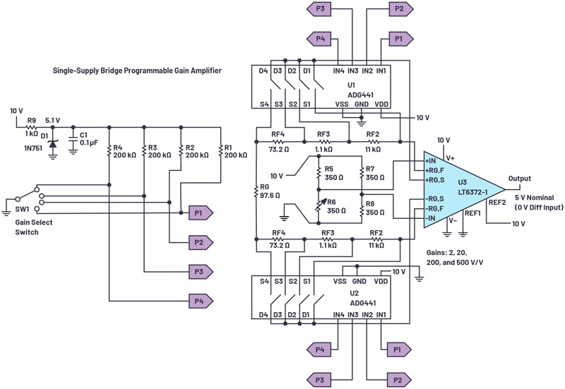
An amplifier like the LT6372-1 from Analog Devices can alleviate these concerns when configured as a PGIA, shown in Figure 3, because of how the RG, F and RG, Spins are separately pinned out. The signal from a Wheatstone bridge, consisting of R5 to R8, is amplified with four user-selectable gain values (SW1) to create a PGIA that varies the RF/RG ratio to get the desired gain.
Furthermore, the U1, U2 analog switch RON is minimized as a source of gain error by placing it in series with the input stage inverting terminal and its feedback resistor. Configured this way, RON is only a small fraction of the total internal 12.1 kΩ feedback resistance and thus has little impact on gain error and drift. Distortion due to switch nonlinearity is also minimized because of the RON value being a small fraction of the overall feedback resistance causing little or no effect due to variation of its value with voltage. Furthermore, the input stage is comprised of a current feedback amplifier (CFA) architecture which allows less variation in bandwidth or speed as gain is varied when compared to a traditional voltage feedback amplifier.1 All this culminates in the ability to create a precision PGIA with accurate gain steps using low cost external analog switches.
Click image to enlarge
Figure 3. PGIA bridge interface with four gain settings
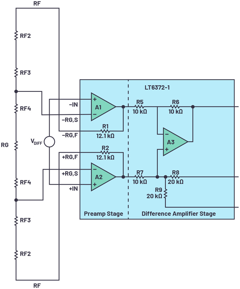
Figure 4 shows a simplified diagram of the PGIA to demonstrate how different taps of the resistor ladder, implemented by analog switches (eight total) shorted two at a time to set the gain, configure the circuit. The two switch banks are depicted in one of the four possible gain values; that being with the–RG, S and+RG, Spins shorted to the RF3/RF4 junction.
Click image to enlarge
Figure 4. LT6372-1 amplifier block diagram and simplified external connection (gains witches not shown) for the PGIA
Design Steps to Compute External Resistors for Any Gain
Figure 3 shows the complete PGIA configuration, including the switches required, which can accommodate an arbitrarily large gain range. Four possible gain values are included here, but it is possible to increase that number by adding more switches. The feature of allowing access to the RG, F and RG, Spins enables one to increase RF for large gains, and to reduce RG for low gains to create a versatile PGIA. For purposes of gain computation, one can consider the feedback resistor to be the internal 12.1 kΩ trimmed resistance plus other resistances in series with RG, F on its way to reach the RG, S terminal. Conversely, the gain setting resistor is the total resistance seen between +RG,S and –RG,S. This is summarized as:
RF= 12.1kΩ + resistance between RG, F and RG, S on each of the two input amps
RG= Resistance between +RG,S and –RG,S
Gains from greater than 1V/V up to 1000V/V are possible with this configuration. With the switches set to short pins S3, and D3 on both U1 and U2 switches, here are the corresponding RF and RG values and the resulting gain:
RF = 12.1 kΩ+ 11 kΩ+ 1.1 kΩ= 24.1 kΩ
RG = 73.2Ω+97.6 Ω+73.2Ω=244 Ω
G=1+2RF/RG =1+2 ×24.1kΩ/244Ω =199V/V
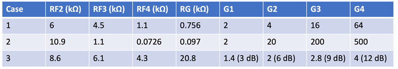
It is easy to see that deciding on which values to use for the external resistors is an iterative and interdependent process where the possible gain values interact and influence the choice of resistors to use. Some common gain value componentvalues are tabulated in Table 1, but a multitude of gain combinations are possible.
Click image to enlarge
Table 1.Component Values for Some PGIA Gain Combinations
The individual resistors in the gain network can be calculated sequentially using Equation 1, which determines the resistors as labeled in Figure 3, where Case 2 from Table 1 (gains 2, 20, 200, and 500V/V) is used as a worked-out example. The feedback resistors and the gain setting resistors are interactive; thus, the formula must be a series where the present term is dependent on the preceding term (s):

Where:
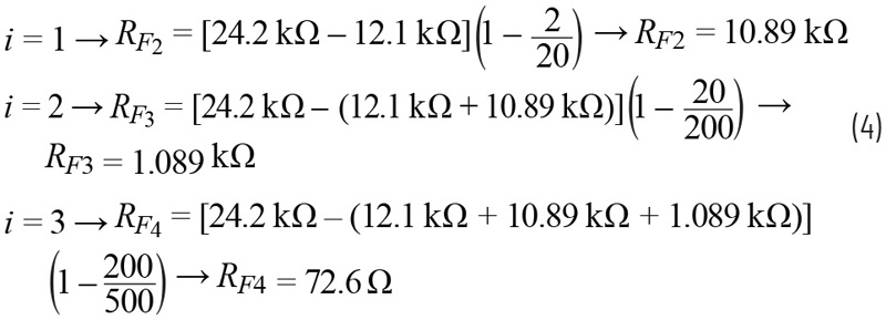
RF1 = 12.1 kΩ (internal to the LT6372-1)M: Number of gains (4 in this case)
Gi: The gain instance (either 2, 20, 200, or 500V/V for G1–G4 respectively of this example)
i:Varies from 1 to (M-1) to compute RFi+1

Equation 1 can be used to calculate the necessary feedback resistors for any set of gains. A dummy variable (j) serves as a counter to keep a running total of the preceding feedback resistors.
Before making any calculations, it is advised to draw a resistor network similar to the network in Figure 3. The network will have (2 × M) – 1 resistors, where M= number of gains. For this example, M=4 and, therefore, the resistor string will have seven resistors. Equation 1 needs to be evaluated for i=1→ (M–1).
G1= 2, G2= 20, G3= 200, G4 =500 V/V
From Equation 2:

Evaluating Equation 1 iteratively from i =1 →(M-1)
The center resistor RG can then be computed using the following:
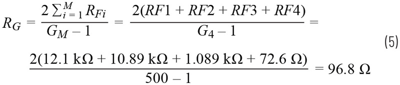
With this last computation, all four resistor values shown in Table 1 are computed and the design computation is finished.
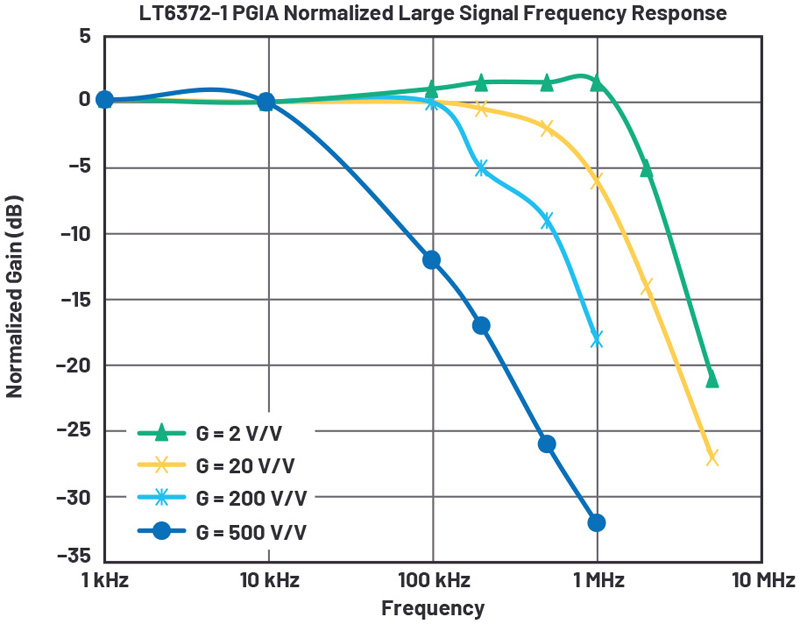
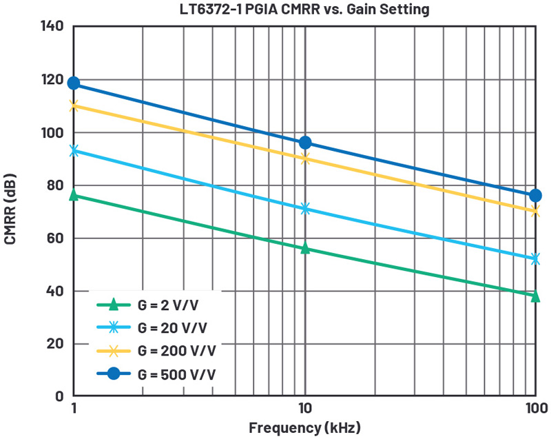
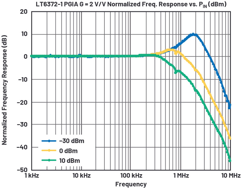
Figures 5 and 6 show the performance that can be achieved with this PGIA configuration:
Click image to enlarge
Figure 5. PGIA large signal frequency response
Click image to enlarge
Figure 6. PGIA CMRR vs. frequency
With the switch capacitances of the ADG444, at the lowest gain setting (G1 = 2 V/V), the small signal frequency response shows some appreciable peaking (see Figure7). This behavior only shows with the lower gain settings where the LT6372-1 bandwidth extends high enough to be affected by the pF range capacitance of the switch. Choosing a lower capacitance switch (for example, ADG611/ADG612/ADG613 with 5 pF on capacitance) or alternatively limiting the lowest gain setting of the PGIA are ways to work around this side effect.
Click image to enlarge
Figure 7. PGIA small signal low gain peaking
1CFA closed-loop bandwidth is inversely proportional to the value of RF, whereas a traditional voltage feedback architecture bandwidth is inversely proportional to the gain (RF/RG).


