.jpg)
Applications using small fast-spinning motors are driving a need for compact drives with high-frequency control loop updates
Motor control applications using small fast-spinning motors such as e-turbos, UAVs, surgical instruments and high-speed pumps, and the advent of SiC and GaN switching transistors, are driving a need for compact drives with high-frequency control loop updates. This paper describes a multi-axis motor and power control platform suitable for academic or commercial research and development. It includes motor and power control kit, FPGA development board and FPGA hardware and software design. It supports integrated power and motor control with PWM time resolution up to 300MHz and control update frequencies of 100kHz or more.
Miniaturization, mass reduction and electrification of existing machines leads to the use of very fast spinning motors of 10-100,000rpm. Applications include electric turbo chargers, quadcopter propellers, surgical instruments and high-speed pumps. For adequate resolution and control of the currents being applied to the motors at these speeds, the frequencies of PWM and control updates need to increase from around 10kHz to around 100kHz.
The IGBT switches used in medium-sized power converters do not switch fast enough or efficiently enough to support 100kHz PWM. MOSFET switches are already capable of switching at these frequencies and are used in small power converters like DC-DC converters and small motor drives, but they are not suitable for high-power applications.
Wide-bandgap semiconductor devices based on SiC and GaN are being developed quickly and provide both very low switching and on-resistance losses and higher-power capability. These devices will reduce the efficiency penalty of switching at high frequency, enabling the high-frequency controllers needed for fast-spinning motors.
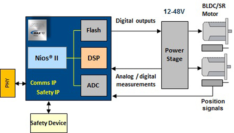
Microcontrollers or DSP chips are often used for embedded control applications. They can be programmed easily and may provide hard interfaces for typical communications and PWM outputs. However, they may also be specialized for a given function so several chips may be required for a typical drive (figure 1).
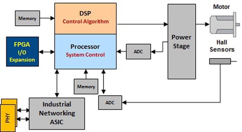
Click image to enlarge
Figure 1: Typical drive block diagram
An alternative method is to use an FPGA (Field-. Programmable Gate Array) to create a system-on-chip including exactly the I/O and processing needed. Such a system-on-chip may use a soft processor or hard processor together with parallel interface IP in the FPGA, for example communicating with industrial Ethernet and safety devices (figure 2). A single FPGA has sufficient I/O to control both power conversion and multi-axis motor control, and can also be used to implement alternative modulation methods to PWM, for example pulse frequency control or hysteresis control, including direct torque control
Click image to enlarge
Figure 2: Communicating with industrial Ethernet and safety devices
In addition to the advantages of integration, FPGAs can be used to accelerate control calculations, for example field-oriented control in PMSM motors or sensor-less speed control using an extended Kalman filter. An FPGA is usually required to achieve control loop updates fast enough to implement direct torque control.
Modern programming tools enable the FPGA system to be composed from off-the-shelf IP components for low-level processing and interfacing, soft or hard processors to run application software, and DSP algorithm IP designed using high-level design tools with automatic code generation.
Intel Drive on Chip reference design is a working example of a system-on-chip FPGA system design. The design is freely available and is compatible FPGA development boards and motor control hardware designed by Intel and its partners.
The reference design comprises:
- Power electronics and motor control kit
- FPGA development board
- FPGA hardware design including NIOS II® processor and IP
- Processor software
· GUI for monitoring and logging signals
A new motor control hardware platform suitable for academic or commercial research and development has been designed by Intel with its partner D3 (figure 3). It includes these features:
- 12V input
- 12-48V DC link generated by bidirectional 2-phase DC-DC converter
- 2x 3-phase motor drives, or 6 half-bridge outputs
- Both analog and digital feedback measurements. Digital signals are provided by ΔΣ ADCs
- Support for Encoder/Resolver/Hall motor position feedback
- MOSFET switching transistors to support 100+kHz PWM
- DC-DC and motor axes controlled by a single FPGA development board connected via its HSMC connector
.jpg)
Click image to enlarge
Figure 3: A new motor control platform designed by Intel & their partner D3
Intel has developed two alternative FPGA architectures, based around the MAX® 10 FPGA, and compatible with the Tandem Motion-Power 48V board’s features. The first uses the NIOS II® processor to coordinate all functions, while the second uses direct data connections between IP components to remove the processor from the control loops, while retaining the processor for higher-level functions.
With the processor-centric design, a memory-mapped interface is used to connect all IP components. The processor is the data master (figure 4). An interrupt from the drive subsystem synchronizes the processor control software to the PWM and ADC readings. The processor’s ISR (interrupt service routine) reads data from interface IP components, performs control calculations in software or via calls to accelerator IP, and writes output to interface IP components, including the DC-DC converter interface and drive subsystem PWM IP. The MAX® 10 ADC interface is connected in addition to the ΔΣ ADCs. The processor reads both ΔΣ and MAX® 10 ADC signals. The user can select which signals to use and view using System Console software provided. The standard PWM frequency is 8kHz and control frequency is 16kHz.
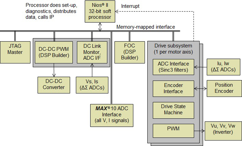
Clcik image to enlarge
Figure 4: In a processor-centric design, the processor is the data master
To achieve higher PWM and control frequencies an alternative architecture was developed (figure 5), and includes a similar set of IP components including the central processor. However, streaming interfaces are used to pass data from the ADC interfaces to a new sample store and router IP, which sends the data directly to the IP components which require it. The processor still uses an ISR to synchronize the reading of data and other operations. There is a central Drive State Machine for start-up and shutdown logic, and multiple drive subsystems, which now include the motor field-oriented control calculations. By reducing the work done by the processor ISR and doing all motor control operations in parallel, the control loop update frequency can be increased from 16kHz to 125kHz, which is set by the MAX® 10 integrated ADC configuration used (2x 1Msample/s ADCs multiplexed to handle 16 feedback signals). Frequencies higher than 125kHz could be achieved with fewer ADC signals or by using external ADCs.
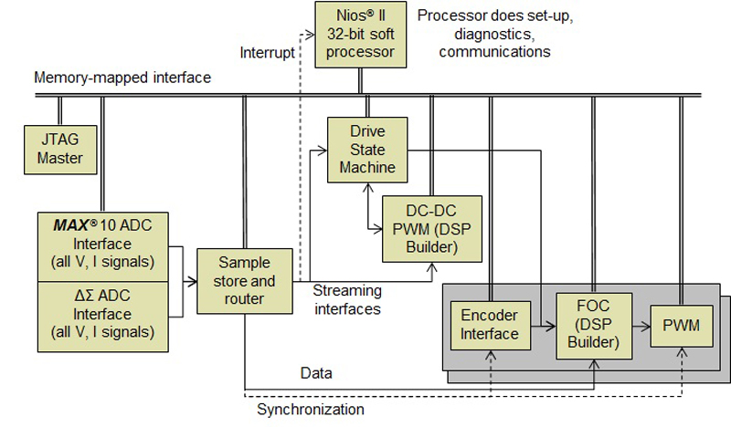
Clcik image to enlarge
Figure 5: Alternative architecture to achieve higher PWM
More use of FPGA parallelism was used in the PWM waveform generation HDL to increase the clock frequency used from 50MHz to 300MHz. This means the PWM switching points can be adjusted in time steps of 3.33ns. The improved resolution may be used for more precise control of new fast-switching transistor types or for improved frequency resolution in designs with variable-frequency PWM, for example resonant power converters.
Intel’s Simulink-based DSP Builder® tool was used to implement alternative implementations of the FOC algorithm with fixed point and variable-precision floating point, and generate HDL code automatically. The tool allows the designer to experiment with different architecture and use folding and alternative precisions to adjust the FPGA resources used and the latency. The latency of all variants is less than 1.5µs, enabling control loop updates of 100+kHz.
The Drive-On-a-Chip reference design for the Tandem Motion-Power 48 V kit (figure 3) uses the FPGA to control a bidirectional DC-DC converter as well as two motors. The DC-DC converter controller, including PWM waveform generation, is also written in DSP Builder®. As well as generating HDL code automatically, the controller can be attached in Simulink to a simulation of the power electronics and load, so a model-based design approach can be used. The standard controller uses a 62.5kHz PWM with cascaded inductor current and load voltage control loops. However, the user can take advantage of the flexibility of the FPGA to redesign the controller, for example using hysteresis control of inductor current instead of PWM to improve the controller response time.
This article has introduced a novel multi-axis motor control and power conversion development platform using a single Intel MAX® 10 FPGA, supporting both processor-centric and high-frequency IP-based control architectures.
The high-frequency design combines a processor-based architecture for diagnostics with low control latency, by
- Connecting FPGA IP components with streaming interfaces to do control loop tasks
- Providing the IP with memory-mapped interfaces for diagnostics as well as streaming interfaces
- Using the processor to collect data from the IP over a memory-mapped interface
The new architecture gives a reduction in latency of 75%, from 93.75µs to 24 µs, with a corresponding 4 times increase in controllable bandwidth, from 1.3kHz to 5.2kHz.
These developments, with the new Tandem Motion-Power 48V motor control board, provide a platform for developing high-frequency (100+kHz control update) multi-axis motor control and power conversion applications.