Accelerating High Power Energy Infrastructure Design
Thanks to its efficiency and size advantages over other semiconductor process technologies, SiC is ideal for use in high-power applications
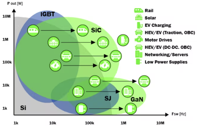
Figure 1: The power, switching frequency, and application use cases of different semiconductor materials (source onsemi)
Power conversion is an essential function in almost every design, from low-power Internet of Things (IoT) sensors to high-power solar inverters. Trends such as using renewable energy sources and the growth of electric vehicle adoption demand efficient and reliable energy conversion. This article highlights some of these trends, explores the electronics engineering challenges, and explains how wide bandgap silicon carbide (SiC) technology has quickly gained adoption.
We focus on one application—a fast DC EV charger—and discuss a typical charger's engineering challenges and high-level architecture. The design considerations of a discrete v. modular approach are discussed briefly, followed by a showcase of the onsemi F1 half-bridge module.
High-Power Energy Conversion Challenges
Power conversion is a broad topic. Power conversion and management is as essential for a battery-powered edge node IoT sensor as it is for a large commercial solar power converter. The difference between them is the level of power involved. The sensor may be only drawing a few milliwatts during operation compared to potentially thousands of watts for the solar power unit. Power conversion is vital in converting from one voltage level to another. For example, the IoT sensor's microcontroller typically sets the voltage requirement, with 3.3V or 5V being popular. However, the nominal voltages of battery chemistry often used for this application provide 3.7V. The same applies to higher power applications such as solar charge converters, uninterruptable power supplies, and electric vehicle chargers. Conversion from one voltage to another is, therefore, required. Despite the vast power differences between these application examples, conversion efficiency is crucial. In high-power conversion applications, an inefficient power conversion results in energy losses that manifest as heat. Too much waste heat requires dissipation to keep the electronic circuitry cool and to work reliably. Dissipating the heat and drawing it away from the power conversion semiconductors is a thermal challenge.
Silicon Carbide Semiconductor Technology
In any high-power power conversion application, the conversion efficiency is primarily determined by the power semiconductors' characteristics. Several properties in a semiconductor result in energy losses occurring inside the device, collectively resulting in heat. Although measuring in milliohms (mΩ), the semiconductor's conduction resistance, RDS(on), can become a significant factor for high-power applications that involve hundreds or thousands of amps. Silicon-based (Si) semiconductor technologies have reached the limit of their thermal and electronic properties, and with an increasing global emphasis on energy efficiency, new semiconductor process technologies have emerged.
Wide bandgap semiconductor process technologies, such as silicon carbide (SiC), offer much improved thermal and electronic properties than silicon, permitting them to operate at higher switching frequencies, higher voltages, and higher temperatures. Figure 1 compares the power handing and switching frequency characteristics of different semiconductor materials and application use cases.
SiC offers many advantages compared to silicon, including an x3 increase in thermal conductivity and an x3 higher energy bandgap. With SiC, applications can use a 1,200V switching voltage compared to 600V with silicon. Perhaps it is no surprise that SiC semiconductors such as SiC MOSFETs are increasingly utilised in high-power power conversion applications, such as EV chargers. SiC devices can also operate at a higher power density, contributing to smaller designs, a feature that is much in demand for space-constrained EV chargers and roadside charging infrastructure.
As SiC process technologies have matured, smaller process nodes deliver smaller and competitivity priced MOSFETs, further accelerating market adoption.
Exploring the Architecture of a Fast DC Electric Vehicle Charger
The availability of widespread charging infrastructure is a critical success factor in the growth of electric vehicles. Onboard chargers provide a simple yet slow method of charging an EV from a domestic supply overnight. To achieve faster charging, DC chargers operate at higher power levels than a domestic supply can supply, requiring considerable electrical infrastructure. Fast DC chargers typically start at 20kW with an anticipated charging duration of two hours. Higher power capacity charging stations extend to 350kW and reduce the charge time to below ten minutes.
Engineers tasked with designing a fast DC EV charger face several development constraints. Above all, EV charging infrastructure is entirely unattended and expected to operate in an outdoor environment subject to rain, dust, and temperature extremes. The reliability of operation is paramount since a driver might become stranded if a charger is faulty in many remote locations with limited charging infrastructure.
High-level design goals are likely to impose strict energy efficiency targets, user safety, and effective thermal management, whatever a location's ambient temperature. An EV charging post must not only accommodate all aspects of power conversion from the mains supply, but also monitor charge, interact with the vehicle's control system, and communicate with the service provider's billing system. Physical space is always at a premium, and mechanical engineers should allocate sufficient space allowance for proper thermal management within the charging station. Charging infrastructure also should comply with all relevant electrical safety, functional safety, and vehicle charging standards (CCS, CHAdaMO, Tesla etc.). Another relevant consideration for high frequency, high power switching converters is compliance with regional and national electromagnetic interference (EMI) standards.
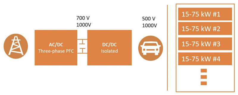
Figure 2 illustrates the basic architecture of a fast DC EV charger. The two principal components are an AC/DC three-phase power factor correction (PFC) or Active Front End (AFE) function and a high-power isolated DC/DC converter. High-power charging stations typically utilise multiple 15kW to 75kW sub-units to achieve the desired capacity.
Click image to enlarge
Figure 2: The architecture of a fast DC electric vehicle charger (source onsemi)
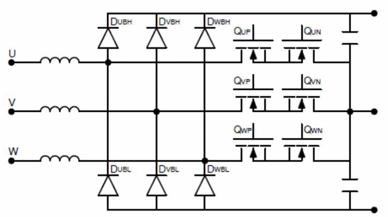
Each functional block may be implemented in a different topology—for example, a T-Neutral Point Clamp (T-NPC) for the PFC boost stage and a full-bridge LLC zero voltage switching (ZVS) for the DC/DC conversion.
Figure 3 illustrates a typical three-phase PFC boost converter for an EV charger using 1,200-volt SiC MOSFET modules in a T-NPC topology.
Click image to enlarge
Figure 3: A typical three-phase PFC stage using a T-NPC topology (source onsemi)
For the DC/DC converter stage, the dual active bridge topology implemented with half-bridge SiC MOSFET modules offers a compact and efficient arrangement.
An Optimal Solution for EV Charging Infrastructure
Although power engineers could build an EV charger's PFC and DC/DC converter stages using discrete SiC MOSFETS, encapsulated SiC MOSFET power integrated modules (PIM) offers space and thermal management advantages. An example is the onsemi NXH006P120MNF2PTG 2-pack SiC MOSFET module. This half-bridge module incorporates a 6mΩ RDS(on)1,200-volt MOSFET and a thermistor in a compact, thermally efficient F2 package (see Figure 4).

Click image to enlarge
Figure 4: The onsemi 1,200V, 10mΩ SiC MOSFET and integrated thermistor in an encapsulated thermally efficient F1 package (source onsemi)
The SiC half-bridge MOSFET module suits solar inverter, EV charging, and industrial power applications.
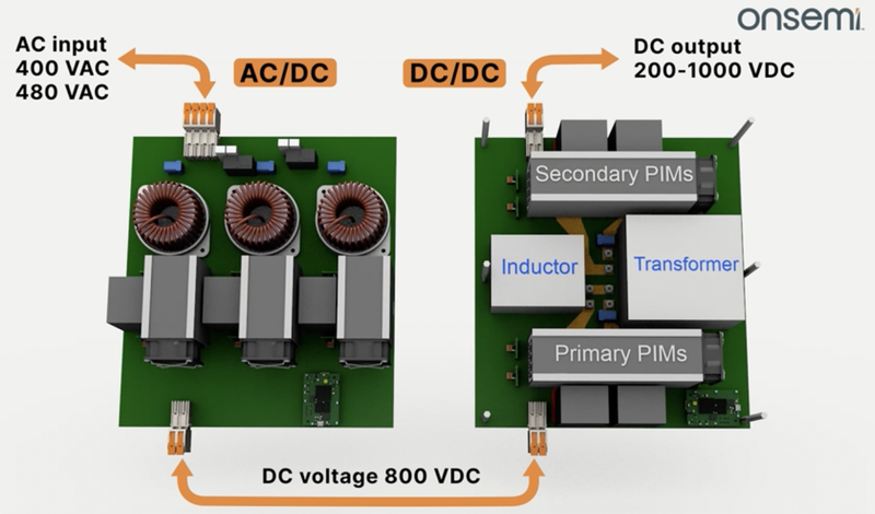
Figure 5 illustrates using NXH010P120MNF1 modules in the PFC and DC/DC converter stages of a 25kW EV charger. The 6-Pack PFC function (left) provides power factor correction and AC/DC conversion, and boosts the DC input voltage to 800V for the DC/DC converter.
Click image to enlarge
Figure 5: The functional architecture of a 25kW EV charger using onsemi NXH010P120MNF1 SiC MOSFET modules (source onsemi)
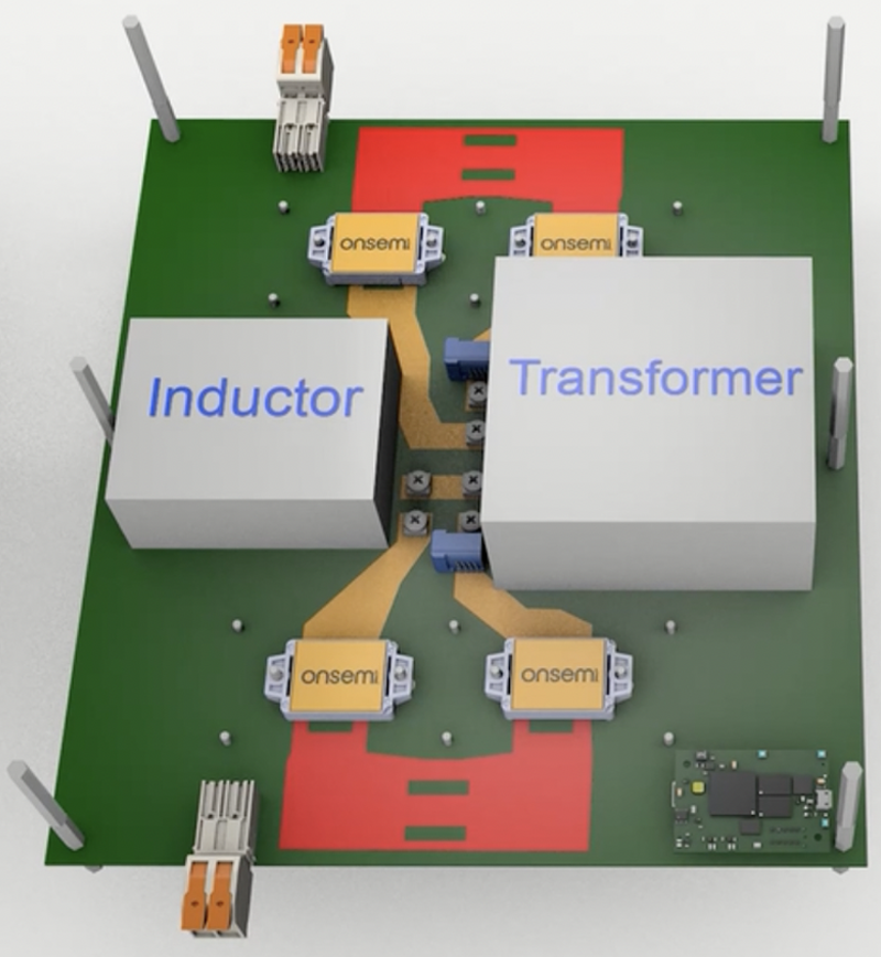
Figure 6 illustrates the dual active bridge arrangement with primary and secondary power integrated modules (PIMs) shown without their heatsinking and forced air cooling fans. The DC/DC converter provides isolation between the vehicle and the three-phase supply and adjusts the output voltage and current as required by the EV's battery management system.
The compact, low RDS(on), thermally optimised, and high-frequency characteristics of the onsemi SiC half-bridge modules make them ideal for high-power EV charging infrastructure applications.
Click image to enlarge
Figure 6: Dual active bridge arrangement with primary and secondary power integrated modules (PIMs) shown without their heatsinking and forced air cooling fans
Accelerating the Development of Efficient Power Conversion Applications
As EV sales continue to grow, the rapid development and deployment of reliable charging infrastructure is crucial. This short article has highlighted how recent advances in semiconductor process technologies have proved silicon carbide-based MOSFETs have superior characteristics compared to silicon counterparts. By packaging multiple SiC MOSFETs into compact, thermally optimised form-factor, engineers can quickly bring high-power conversion applications to market.