Flyback converters are favored for their simplicity and low BOM cost. The active clamp flyback topology significantly boosts conversion efficiency and enables greater power density, which can be further increased when combined with GaN’s superior switch
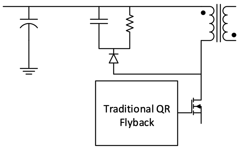
Figure 1. Traditional QR flyback converter with protective RCD clamp
Flyback topologies are often chosen for AC/DC conversion in low- to medium-power applications such as USB adapters and battery chargers. Among their inherent strengths, the transformer-based design provides galvanic isolation and facilitates a wide input voltage range. Moreover, the simplicity of the topology and its associated low BOM cost allow power supplies to be compact, lightweight, and competitively priced.
Basic flyback converters typically operate in discontinuous conduction mode (DCM) with hard switching, which causes losses to be high and generates electromagnetic interference (EMI). This discourages the use of higher operating switching frequencies to reduce the size of magnetic components and increase power density.
One solution has been to adopt the quasi-resonant (QR) flyback topology, which operates with valley switching that lowers losses as well as EMI. This lets flyback converters retain their simplicity, while efficiency can be as high as 90-91% with silicon MOSFETs. However, although losses are significantly lower than in the hard-switched topology, switching losses are incurred because valley switching happens at non-zero voltage. Also, the losses increase with frequency so QR converters are typically operated below 100 kHz.
A better solution is needed to satisfy ongoing demands to raise efficiency further while also increasing power density. Driving these demands are the evolution of specifications such as USB Power Delivery (USB-PD), which first raised the power delivered over USB Type-C cables to 100 W and later further increased the limit to 240 W. to serve the market for these adapters, greater power density is a perennial quest. Small size is important to buyers, who typically look for portability to be able to charge their devices on the go and will seek a convenient adapter to carry in a pocket, bag, or travel kit. Also, smaller adapters help minimize clutter in charging stations or desk setups and align with the overall trend towards slim and minimalist accessory designs that complement the aesthetics of users’ gadgets.
To address this, the active clamp flyback (ACF) converter further reduces switching losses and allows the use of higher frequencies - hence smaller magnetic components for greater power density - without compromising efficiency or EMI.
Protective Clamp Principle
A traditional flyback converter needs a resistor capacitor diode (RCD) clamp (figure 1), to provide a path to dissipate the energy stored in the transformer leakage inductance. This protects the converter’s main power switch from electrical overstress associated with drain voltage spikes during turn-off events. Unfortunately, power losses in the RCD clamp components impair overall system efficiency and generate unwanted heat. The losses increase with switching frequency.
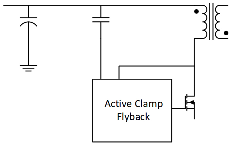
The ACF topology (figure 2) differs from the traditional flyback converters by re-using energy stored in the transformer’s leakage inductance that would normally be dissipated in the passive clamp components. Supplying this ‘recycled’ energy to the load during the switching cycle improves converter efficiency.
Click image to enlarge
Figure 2. An ACF controller integrates active clamp circuitry, including clamping MOSFET, on-chip
The active clamp consists of a clamp switch (MOSFET) and a clamp capacitor, which replaces the passive RCD clamp. The clamp MOSFET provides a path for the energy from the transformer leakage inductance to be stored in the clamp capacitor and thus protect the main flyback-converter switch from electrical overstress. The energy dissipated due to on-resistance (RDS(ON)) of the clamp MOSFET is close to zero, compared to the losses associated with the forward voltage (VF) of the conventional passive diode. Moreover, the MOSFET’s ability to allow bidirectional clamp current permits leakage energy to be returned to the transformer on every switching cycle and thereby passed to the load instead of being wasted.
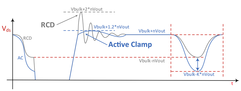
Also, the quasi-resonant (QR) valleys in the ACF converter are significantly lower than a passive clamp circuit will allow (figure 3), often practically achieving near-ZVS operation. Thus, the active clamp topology is almost lossless, with greatly reduced EMI, and maintains high efficiency with increasing switching frequency.
Click image to enlarge
Figure 3. Lower drain-voltage spikes and near zero-voltage switching with ACF converter
In addition, reducing the peak voltage across the primary switch during the turn-off events allows a more aggressive turns ratio between the primary and secondary winding of the transformer. This allows a lower voltage rating for the synchronous-rectifier switch on the secondary side, which gives the designer more opportunities to reduce the overall system cost and/or specify lower on-resistance and reduced conduction losses.
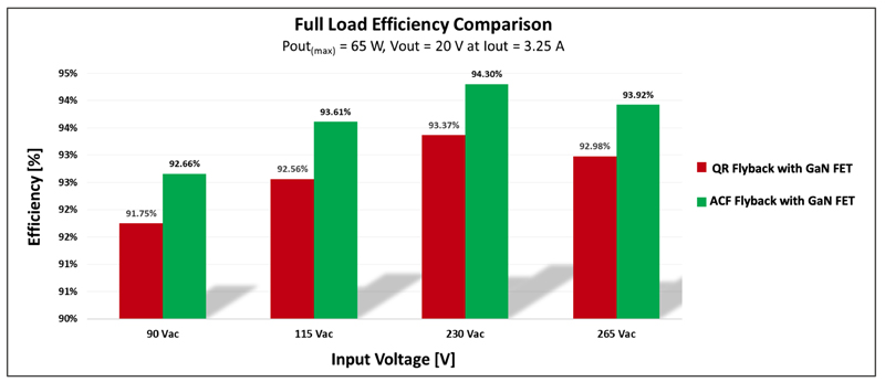
Comparison with QR converters has shown that the ACF topology reduces power losses by about 20%, by recycling the leakage energy of the transformer and greatly reducing the switching losses. Figure 4 shows how the efficiency can be improved across the universal input (90-265 Vac) line voltage for a 65 W power adapter using ACF instead of QR flyback.
Click image to enlarge
Figure 4. Typical efficiency improvement enabled by ACF converter.
Although the efficiency improvements in absolute values may appear marginal they actually represent a significant reduction in system losses. For example, at 230 Vac, improving the efficiency from 93.37% to 94.3% corresponds to saving more than 14% of losses. This directly translates into lower thermal dissipation which practically allows reducing the size of the adapter without increasing the case temperature. Experiment shows that this 0.91% efficiency improvement translates into a significant 12 oC touch temperature improvement for a 65 W power adapter.
ACF and GaN
ACF is widely recognized as being more efficient than the QR flyback topology. More recently, wide-bandgap gallium nitride (GaN) high electron mobility transistors (HEMTs) have become commercialized and shown to incur significantly lower switching losses than comparable silicon power devices. Also, with zero reverse recovery, GaN HEMTs can operate efficiently at higher switching frequencies and so allow a further reduction in magnetic component sizes in pursuit of greater power density.
Bringing together the ACF topology and GaN wide-bandgap technology sets the scene for further improvements in the efficiency and power density of USB-PD adapters and similar accessories. Silanna semiconductor has evaluated two reference designs built with the company’s SZ1131 ACF controller, which allows accurate assessment of the impact of GaN technology on the performance of ACF converters suitable for use in USB-PD adapters.
The SZ1131 is a technology-agnostic ACF controller that can handle a state-of-the-art silicon superjunction MOSFETs or GaN device with minimal circuit modification, helping to achieve an accurate comparison of the two approaches.
Each reference design describes a 65 W offline power supply with universal input and programmable output voltages of 5 V/3 A, 9 V/3 A, 15 V/3 A, and 20 V/3.25 A. The controller implements Silanna’s OptiMode™ cycle-by-cycle adaptive digital control and supports operating frequency up to 140 kHz.
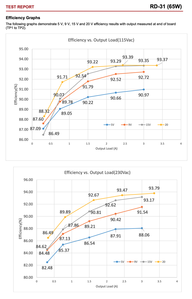
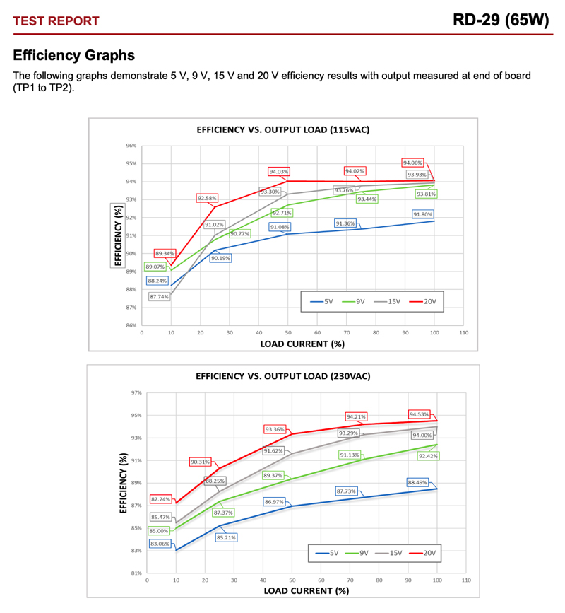
The silicon-based example utilizes a 650 V superjunction MOSFET with 15 A rated drain current, 220 mΩ RDS(ON) and 24.7 nC typical total gate charge (Qg). On the other hand, the GaN design features the Transphorm TP65H300G4LSG 650 V 240 mΩ SuperGaN FET, which has Qg of only 9.6 nC. Thus, the GaN device has superior RDS(ON) x Qg figure of merit (FoM) compared to the superjunction MOSFET.
Figures 5 and 6 compare the efficiency of the superjunction and SuperGaN designs from 10% load to full load. The GaN-based converter reaches maximum efficiency of 94.53% at full load, with 20 V output. This compares with 93.79% for the all-silicon design under the same output conditions. The GaN converter’s efficiency is superior across the load range and for all output voltages.
Click image to enlarge
Figure 5. ACF efficiency with superjunction MOSFET
Click image to enlarge
Figure 6. ACF efficiency with GaN device
The improvement achieved by changing from GaN to silicon in the ACF converter is similar to the improvement achieved by moving from QR to ACF topology. Moreover, GaN technology allows further improvements in power density by using higher switching frequencies that allow smaller magnetic components.
Conclusion
ACF is today’s most efficient flyback converter topology, achieving close to zero-voltage switching while also recycling the leakage energy which would otherwise be dissipated in a passive clamp circuit to protect the converter’s main power switch. In this way, the active clamp saves about 20% of switching energy, which boosts efficiency and significantly lowers power-adapter case temperature.
Combining the inherently greater efficiency of the ACF circuit with the superior FoM of GaN power semiconductors permits a further significant increase in efficiency by adopting wide-bandgap technology in the latest ACF designs. Moreover, the inherently lower EMI of the ACF topology and the potential for GaN devices to operate at higher switching frequencies provides further opportunities to reduce the size of magnetic components and increase power density without increasing losses or EMI.