Achieving High Power Density in a Regulated IBC for Data Center Applications
The current approach and Infineon’s novel regulated DR-HSC topology
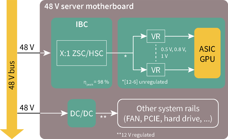
Figure 1: 48 V server architecture in a typical data center
Introduction
Approximately half of the energy consumed in a typical data center is wasted, either during power conversion or through cooling. Given the increasingly urgent requirement to reduce CO2 emissions, this undesirable situation required addressing at both system and converter levels. Research [1] indicates that using 48 V power distribution at the rack level would help to reduce power losses, and this approach is now widely adopted. 48 V distribution enables a more efficient way to transfer power to the payload (i.e., ASIC/CPU/GPU), where a two-stage approach is commonly adopted. The first stage is the intermediate bus conversion from 48 V to 12 V and the second from 12 V to lower voltage levels.
However, there is a significant gap between the full-load efficiencies attainable using unregulated and regulated converters. This limits the use of higher power density solutions when stepping down from 48 V to 12 V. This article presents Infineon’s novel regulated topology for implementing a regulated intermediate bus converter (IBC) that allows much greater power density in data-center applications.
48 V architecture at server motherboard level: the current two-step approach
The first stage (48 V to 12 V) commonly employs either a resonant converter, such as an LLC, or a switched tank converter (STC). In contrast, the second stage typically uses a multi-phase buck topology. It has been shown that switched capacitor converters can be used to achieve high power density with a 4:1 ratio. In contrast, LLC resonant converters are widely used for IBC because they allow zero voltage switching (ZVS) operation on the primary side and zero current switching (ZCS) operation on the secondary. However, in situations where regulation is required, LLCs start to drift away from resonant operation, leading to a decrease in conversion efficiency.
Figure 1 shows the server architecture currently used in a typical data center. Here, an unregulated voltage rail (6-12 V) provides power for low voltage, high-current components (GPU, ASICs, etc.) while a regulated 12 V rail supplies high-power (600 W to 1.2 kW) peripherals like HDDs, fans, and PCI-E.
Existing solutions use conventional fourth-brick and eighth-brick power modules, but these are large and bulky and cannot provide the power density required by newer and more advanced systems. One of the main limitations of these solutions is that they use bulky magnetic components (i.e., a transformer and inductors). This application’s additional requirement for high peak-power capability makes the inductor-based solution even less attractive. However, where regulation is required, this cannot be avoided.
Novel topology for a much greater power density
Infineon addressed this power density problem by developing a two-stage, dual-regulated, hybrid-switched capacitor converter (DR-HSC) topology, which formed the basis for a new two-stage IBC converter design (Figure 2).

Click image to enlarge
Figure 2: Infineon’s two-stage, dual-regulated, hybrid-switched capacitor converter (DR-HSC) topology
The first stage comprises a half-bridge multi-level structure and resonant capacitor, with an additional inductor (LZVS) in series with a DC blocking capacitor (CC) to enable zero-voltage switching operation for all the FETs. The second stage includes two multi-level half-bridges where their phase nodes are shorted and controlled with a 180° phase shift. An additional balancing inductor, Lbal, can be placed between the two positive or negative terminals of the flying capacitors (Cfly1, Cfly2).
The first stage operates in an open-loop mode and divides the input voltage in half by running at high frequency and with LZVS enabling zero-voltage switching (ZVS) operation for all first-stage switches. The second stage is controlled so that for one part of the switching-cycle TSW, Cfly1 and Cfly2 are connected in series between the input voltage Vout1 and GND. This ensures that the sum of both flying capacitors always equals the input voltage, Vin.
However, there is no guarantee that the connection at the midpoint of the two flying capacitors is balanced under all conditions (e.g., mismatched driver propagation delays). Therefore, to enforce balancing, it is possible to include an inductive component. Soft-switching in the first stage high-voltage domain provides high permeances for the whole system. In contrast, low-frequency operation with hard switching enables second-stage regulation with almost no current ripple in the output inductor. As a consequence, the topology ensures the best use for both stages.
Figure 3 shows the main operation waveforms of the 2:1 ZSC stage (a, left) and the second stage main waveforms (b, right) for DR-HSC topology. It is interesting to analyze the proposed DR-HSC topology for different duty cycles. The sweet spot is at 50 percent duty cycle: in this operation mode, the phase voltage node of the three-level flying capacitor (3LFC) is equal to the output voltage when 48 V is applied. This means the current ripple in the output inductor is almost zero, which is very important, this being the nominal condition in a 48 V to 12 V converter.
.png)
Click image to enlarge
Figure 3: DR-HSC main operation waveforms for the 2:1 ZSC stage (a) and the second stage (b)
.png)
Click image to enlarge
Figure 3: DR-HSC main operation waveforms for the 2:1 ZSC stage (a) and the second stage (b)
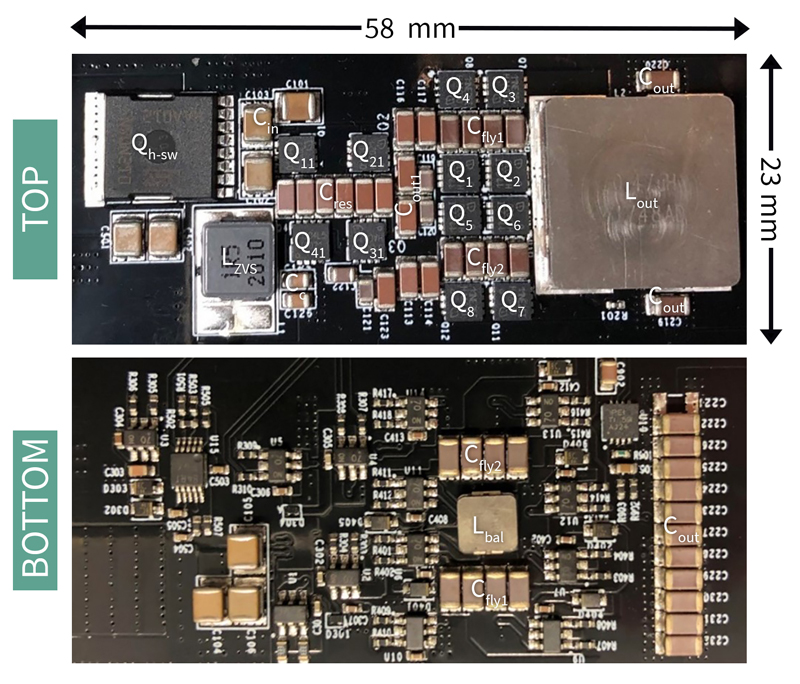
Switching devices used in this design are low-RDS(ON) OptiMOS™ Source-Down 40 V and OptiMOS™ power MOSFET 25 V using EiceDRIVER™ 1EDN gate drivers. The used controller is the XDP™ XDPP1100 digital power controller – a mixed-signal SoC optimized for isolated DC-DC power applications. It includes a high-performance analog front-end, a state machine-based digital control loop, and a microcontroller, all integrated into a single chip. The evaluation board for the DR-HSC topology is shown in Figure 4.
Click image to enlarge
Figure 4 : Evaluation board of DR-HSC 48 V-to-12 V converter
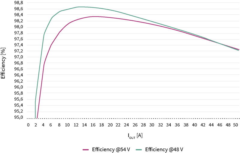
The DR-HSC test board has achieved over 98 percent peak efficiency and above 97 percent at full load (Figure 5).
Click image to enlarge
Figure 5: DR-HSC efficiency vs. load current
One of the critical enablers for achieving high efficiency and high power density is to use MOSFETs with a low-voltage rating. However, the start-up can be a concern with these devices. In a zero voltage switching switched-capacitor converter (ZSC), to allow the safe use of low voltage class MOSFETs, a hot-swap circuit at the input is required to soft-charge all resonant and output capacitors. An essential component in the hot-swap circuit is the linear FET, which operates in the linear region during start-up. This limits the inrush current to a safe level so that the input voltage ramps up to slowly charge all capacitors in the circuit to their target value without stressing the low voltage MOSFETs.
Conclusion
Infineon has proposed DR-HSC, a novel 48 V to 12 V regulated topology which can be combined with OptiMOS™ technology, EiceDRIVER™ 1EDN gate driver for MOSFETs, and XDP™ XDPP1100 digital controller to create a high performance and robust solution with the high level of power density required by IBCs in data center applications.
Find more information on Infineon’s ecosystem for data centers here.
References
[1] M. Dayarathna, Y. Wen and R. Fan, “Data Center Energy Consumption Modeling: A Survey,” in IEEE Communications Surveys & Tutorials, vol. 18, no. 1, pp. 732-794, Firstquarter 2016, DOI: 10.1109/COMST.2015.2481183
[2] S. Jiang, S. Saggini, C. Nan, X. Li, C. Chung, and M. Yazdani, “Switched Tank Converters,” IEEE Transactions on Power Electronics, vol. 34, no. 6, pp. 5048-5062, June 2019, DOI: 10.1109/TPEL.2018.2868447.
[3] C. Rainer, R. Rizzolatti, and D. Varajao, “High-Density Cascaded ZVS Switched Capacitor Converter for 48-V Data-Center Application,” PCIM Europe digital days 2020; International Exhibition and Conference for Power Electronics, Intelligent Motion, Renewable Energy and Energy Management, 2020, pp. 1-8.