Active Front End Rectifier
Design tips for making the best SiC power topology and modulation decisions
1: Introduction
Battery chargers for electric vehicles require galvanic isolation between the grid connection and the batteries. Therefore, an EV charger almost always has two stages: a high power-quality rectifier that converts AC to DC, followed by a DC-DC converter utilizing a high-frequency transformer for galvanic isolation. The high switching frequency of SiC FETs and diodes can meet charger requirements using “old” and simple circuit topologies that were impractical with silicon-based switching devices. Examples include a totem-pole power factor corrector (TPPFC) for single-phase rectification, and the ubiquitous 2-level voltage source inverter (2L-VSI) for a three-phase rectifier. This article provides an overview of some of the many three-phase rectifier options, a glimpse at modulation options, and power semiconductor loss comparisons.
2: Topology Selection
Suppose we need to design a 22 kW three-phase rectifier, a.k.a. active front end rectifier (AFE) for 400 or 480 VAC line-line RMS. Implied is power factor correction, but power flow can be unidirectional. Cost, harmonic distortion, efficiency, size, and weight are important design criteria. To achieve low harmonic distortion, active power factor correction is required.
For anyone experienced with single-phase PFC, three independent boosters could be an attractive option. Two of many possible implementations are shown in Figure 1.
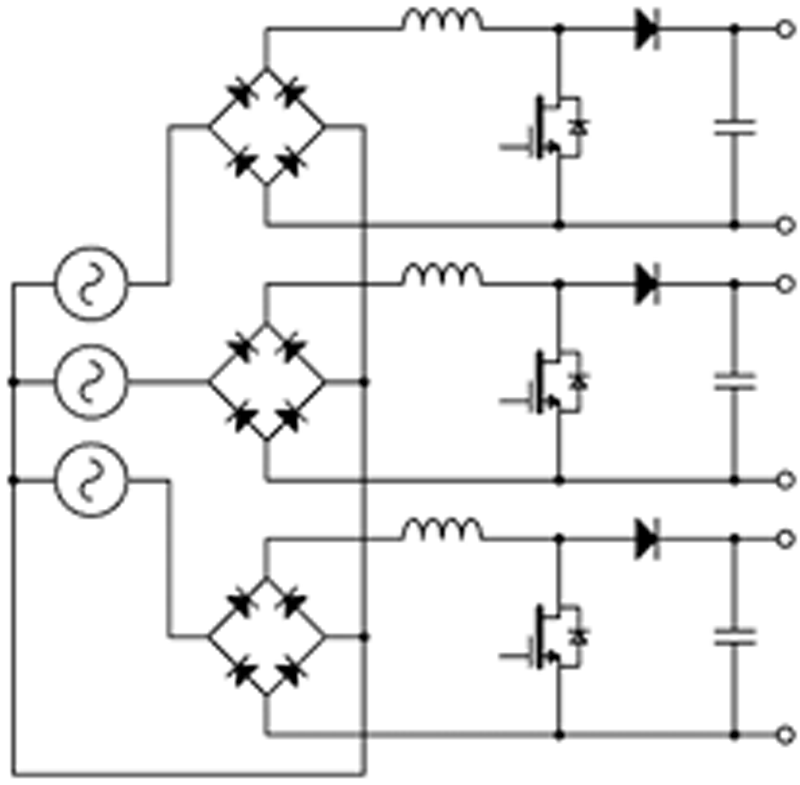
Click image to enlarge
Click image to enlarge
Figures: 1(a) Triple PFC, (b) triple TPPFC
In an EV charger, each booster must supply power to a separate isolated DC-DC converter, the outputs of which are paralleled together. This is a viable approach. The conventional PFC booster efficiency can be improved slightly by eliminating the input diode bridge and using a totem pole topology, an example of which is shown in Figure 1(b). Twelve power semiconductors (some could be diodes instead of FETs) make this approach less attractive considering the same number of devices can yield the benefit of lower cost, smaller line filters in a three-level topology.
Click image to enlarge
Click image to enlarge
Figures 2:Two simple but nonviable topologies: (a) booster following diode bridge, (b) line inductors with booster
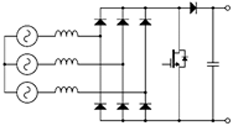
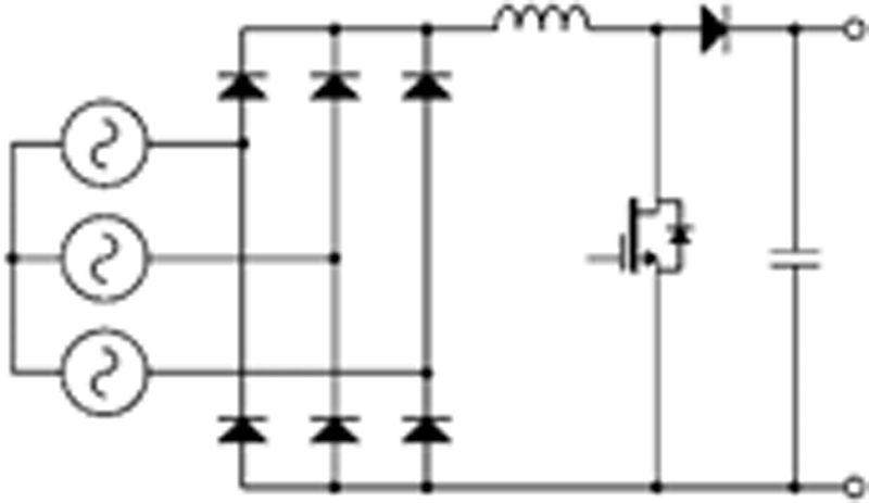
A three-phase diode bridge preceded by three line inductors is obsolete because of high distortion, size, weight, and cost. Adding a boost switch and diode after the three-phase diode bridge, as in Figure 2(a), would shrink the inductors due to the much higher switching versus line frequency. However, this would only work well in certain corner cases due to distortion and so is nonviable. In Figure 2(b), a single booster after the diode bridge, as in a conventional single-phase PFC, yields unacceptable harmonic distortion, about 30%. It is necessary to actively shape each phase current. One of many ways to accomplish this is to add back-to-back FETs connected between each line inductor and a split DC link, as in Figure 3(a). This is a popular variation of the 3-level Vienna rectifier, which is highly efficient with all SiC power semiconductors [1].
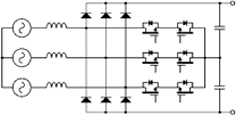
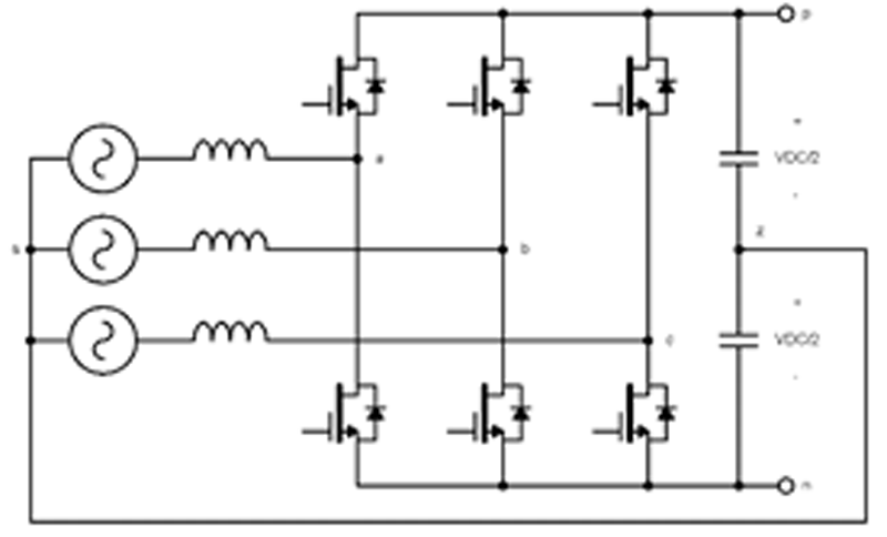
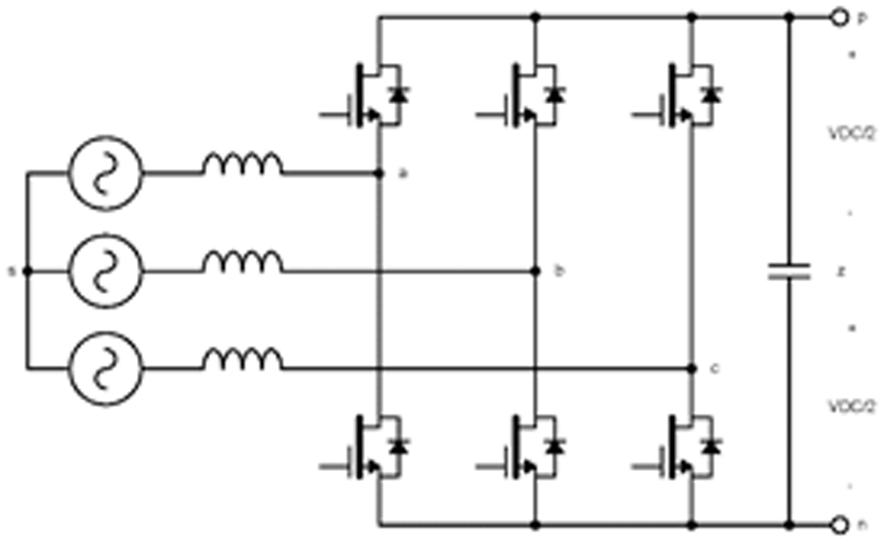
With 480 VAC line-line input, SiC diodes in the Vienna rectifier are 1200 V rated and yet have negligible switching loss. Each diode commutates with its corresponding FET pair at the FET switching frequency. Each FET must block only half the DC link voltage, so switching loss is low, and 650 V or higher FET voltage rating is acceptable. Current is fully shaped in the Vienna rectifier, resulting in very low harmonic distortion. Being 3-level, the line filter is lower cost, size, and weight. Power flow is unidirectional. To support bidirectional power and slightly reduce conduction loss, the diodes are replaced by 1200 V FETs in the three-phase bridge, as in Figure 3(b).
Click image to enlarge
Click image to enlarge
Figures 3: (a) Modified Vienna rectifier, (b) three-level TNPC
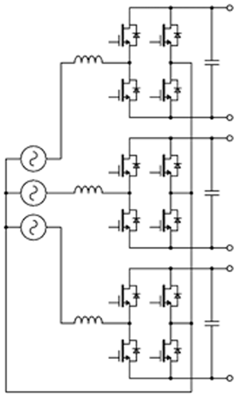
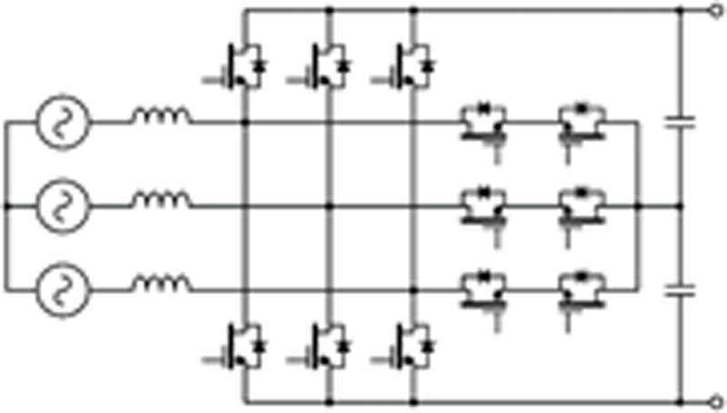
This is the three-level transistor neutral point clamped topology (3L-TNPC). It can operate at any power factor, but when operated as a rectifier, there is negligible switching loss in the bridge FETs. The PWM strategy for 3L-TNPC is inverting pairs of bridge and clamp FETs. As in the Vienna rectifier, each clamp FETs block only half the DC link voltage, so switching loss is low. In some cases, the reduced cost of the three-level line filters is outweighed by the additional FETs and gate drivers. This is solved by simply eliminating the clamp FETs, resulting in the ubiquitous two-level voltage source inverter (2L-VSI). The 2L-VSI has only six FETs, yet it can fully shape the line current with any power factor, so it supports bidirectional power flow and has low harmonic distortion.
Three-level NPC and ANPC topologies could be used, but for this application these offer no advantage over TNPC, especially, with the high performance of SiC FETs. These topologies are needed more for working with higher DC link voltages, for example in solar systems with 1500 VDC input.
3: Modulation Methods
The following derivation focuses on the 2L-VSI, but these modulation methods apply to 3L-TNPC and other inverter topologies.
Click image to enlarge
Click image to enlarge
Figures 4: (a) Half-bridge, (b) sine-triangle reference and carrier waveforms
In a half-bridge, the maximum output voltage referenced to the DC link midpoint z (may be imaginary) using sine-triangle modulation is  as is evident in Figure 4(a). This is true regardless of the number of phase legs because each leg is independent of the others with sine-triangle modulation. In other words, there is no switching coordination between phase legs. This means that a 3-phase, 4-wire connection is straightforward to use, as shown in Figure 5(a).
Click image to enlarge
Click image to enlarge
Figures 5: 2L-VSI (a) with 4-wire connection, and (b) with 3-wire connection
In the 3-wire connection, as in Figure 5(b), the DC link midpoint z is usually imaginary because film capacitors can support the DC link voltage without series connecting them. One advantage of a 4-wire connection in an onboard EV charger is the ability to operate with a single-phase input or a three-phase input. With a single-phase input, two phase legs can operate the same as in a TPPFC.
Click image to enlarge
Figure 6: Three-phase voltage division
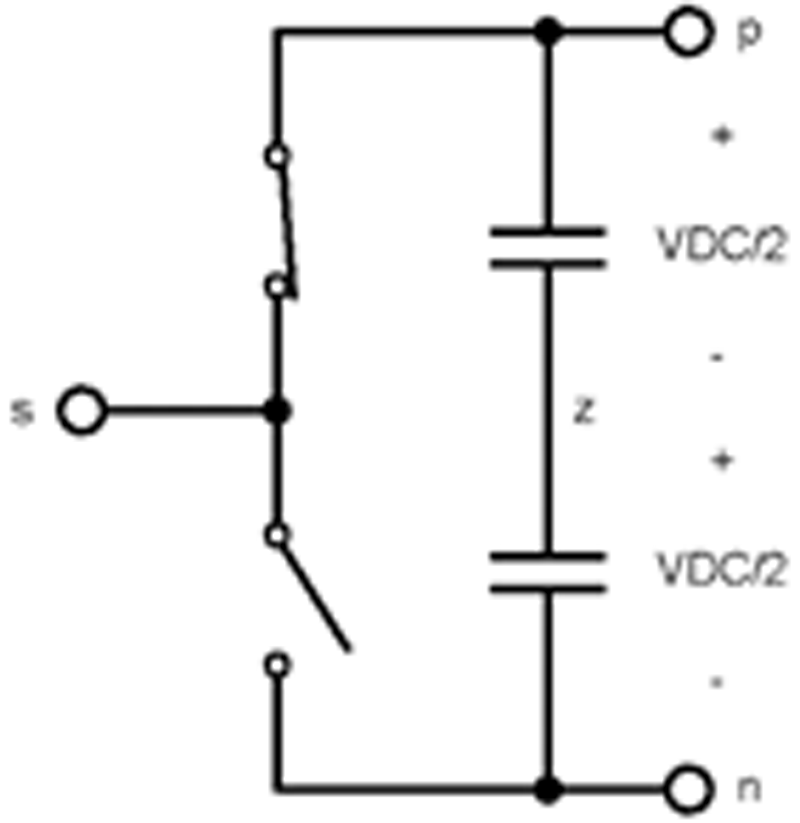
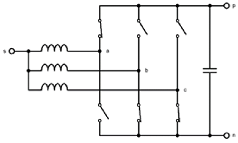
We need to know the range of AC to DC link voltages. One way to derive the maximum line-to-line voltages is by voltage division. With the phase A top switch on and phases B and C bottom switches on, the line-to-neutral voltage of phase A, meaning the voltage from point a to point s in Figure 6 is the DC link voltage (voltage across the capacitor, from p to n) times the impedance of phase A divided by the impedance of phases B and C in parallel (half that of phase A) plus phase A impedance. So, the phase A line-to-neutral voltage is 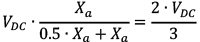 . This is the maximum voltage that can be generated or supported across a load or source. Inserting a balanced three-phase voltage source between the inductors and point s yields the same result because the voltages sum to zero. Using the simple PWM strategy of switches always in opposite states in each phase leg (disregarding deadtime), we create a space vector map by orrelateng the switch combinations with voltage vectors at the AC terminals of each leg.
Click image to enlarge
Click image to enlarge
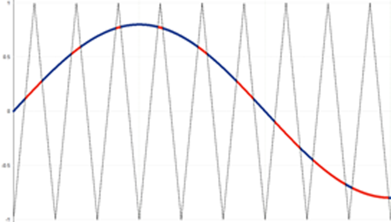
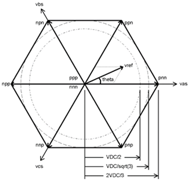
Figures 7: (a) Space vector map for 2L-VSI, (b) sampled waveforms for sine-triangle in red, space-vector in blue, and 60 °C discontinuous modulation in green
The switch states in Figure 7(a) are designated by three letters (or digits), one for each phase, with the letter p or n (or the number 1 or 0) corresponding to the DC link rails in Figure 6. For example, phase A top switch on and phases B and C bottom switches on is designated by pnn. There are eight total vectors for a 2L-VSI: six maximum-voltage vectors and two redundant zero vectors. Line voltages approximate a rotating reference voltage vref by averaging the time spent in vectors near the reference voltage. Dwell times can be calculated using a space vector map as in Figure 7(a), or by comparing reference and carrier waveforms as in Figure 7(b). There is much literature about this [2], but this article touches only on sine-triangle, conventional space vector (centered, and referred to hereafter as SVM), and 60 ° discontinuous modulation (clamp at voltage peaks, also known as DPWM1).
To avoid clipping (pulse skipping) and a jump in harmonic distortion, the reference vector length is limited to the inner circle in Figure 7(a) for sine-triangle, and to the larger circle for SVM and DPWM1. What is the physical reason for the increased magnitude of SVM and DPWM1 voltages? It is because these modulation methods (and others including 3rd harmonic injection) cause the average voltage of node s to “wiggle” at 3x the fundamental (line) frequency with respect to the DC link. This is enabled by sharing time in the zero states between phases. The moving potential of node s “flattens” the SVM and DPWM1 reference waveforms, allowing the factor of 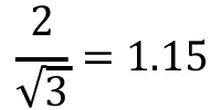 higher line-line voltage for a given DC link voltage compared to sine-triangle. On the other hand, each phase is independent of the others with sine-triangle modulation, allowing the voltage of node s to be fixed with respect to the DC link without changing the modulation and thus facilitating an optional 4-wire connection.
SVM and DPWM1 have the advantages of reduced EMI and wider input/output voltage range. SVM and sine-triangle have almost identical conduction and switching loss in the power semiconductors. DPWM1 has the advantage of reduced switching loss due to clamping to a DC link rail during a 60 ° interval twice during each fundamental line cycle. This advantage often outweighs the increase in conduction loss, even with fast switching SiC.
Sine-triangle and SVM can readily be used with the Vienna rectifier. One can imagine that the Vienna rectifier inherently has discontinuous PWM because of the diode bridge, further enhanced by practically zero switching loss in SiC diodes. It is possible to use a more limited discontinuous PWM of the clamp FETs, but the switching loss in these is already quite low and so is not considered here.
A word about implementation: it is arguably easier to implement a comparison of SVM and DPWM1 reference waveforms as in Figure 7(a) against a triangular carrier waveform (PWM counter) in a microcontroller than to compute PWM dwell times using a space vector map. The jumps in the DPWM1 waveforms will not cause distortion in line currents if the jumps occur simultaneously because the phase voltages always sum to zero. This can be implemented by writing to “shadow” PWM registers, which subsequently update to the active PWM registers on the same clock edge.
4: Efficiency Comparison
Power loss is estimated using the online FET-Jet Calculator tool. For each topology, the numbers of legs or phases is 3. The following conditions apply.
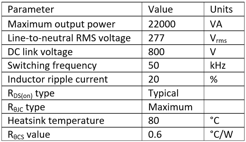
Click image to enlarge
Table 1: Power loss calculation parameters
Click image to enlarge
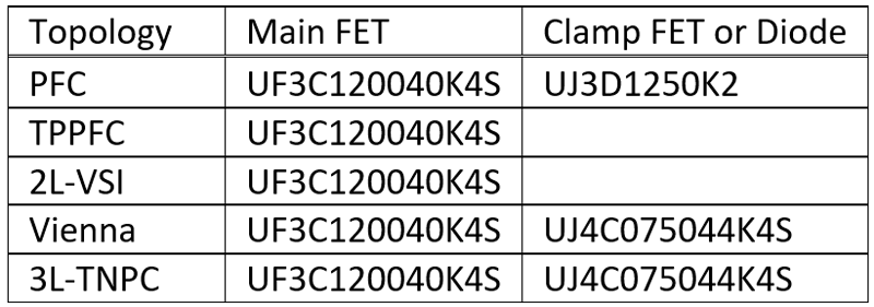
Table 2: Power semiconductor selection
The device selections in Table 2 Power semiconductor selection are made with cost in mind. Slightly lower power loss is possible in some cases with a different device selection. Therefore, many part numbers are offered, so that tradeoffs can be optimized according to various application requirements.
For the PFC, the online calculator ignores the silicon-based line rectifier loss since these are not supplied by UnitedSiC. Therefore, a custom calculation is made that includes the loss of a typical 1200 V single-phase rectifier bridge, KBPC5012FP by Diotec Semiconductor. The results are shown in Figure 8.
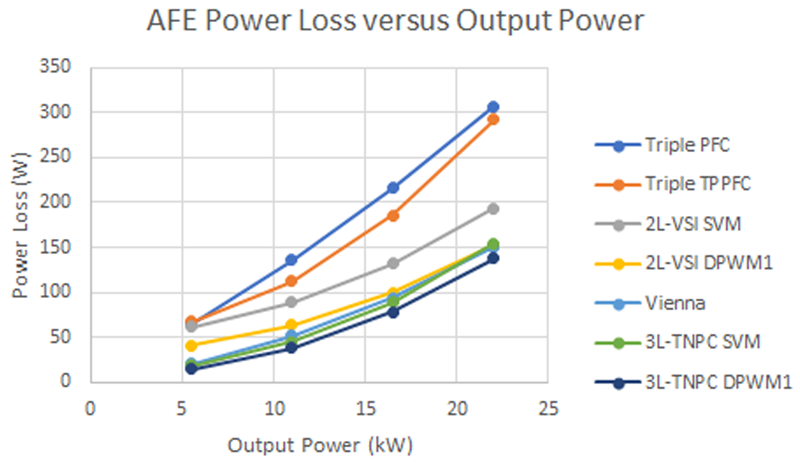
Click image to enlarge
Figure 8: Power loss comparisons
Not surprisingly, the triple PFC has the highest loss, followed closely by TPPFC. This is mostly because of the number of semiconductors in the current path. Next down is 2L-VSI with space-vector modulation. This is also expected because there are only 6 power semiconductors total, and higher efficiency generally requires more hardware. An interesting exception to this is the significant reduction in power loss with discontinuous PWM versus sine-triangle or SVM in the 2L-VSI. The Vienna rectifier beats the 2L-VSI with DPWM1 except at full power where they are roughly equal in power loss. The 3L-TNPC with SVM has only slightly less power loss than the Vienna rectifier, and it is noticeably more efficient with DPWM1.
These results are gathered in only minutes. Further optimizations can be made, and it is reasonable to expect some difference between calculations and actual results. Disclaimers aside, the trends are clear and helpful to guide topology and modulation decisions, and at the very least to eliminate options that are nonviable and focus instead on those that are likely to perform well.
5: References
[1] J.W. Kolar, T. Friedli, “The Essence of Three-Phase PFC Rectifier Systems”, Proceedings of the 33rd IEEE International Telecommunications Energy Conference (INTELEC 2011), Amsterdam, Netherlands, October 9-13, 2011
[2] C. Grahame Holmes, Thomas A. Lipo, “Pulse Width Modulation for Power Converters, Principles and Practice”, IEEE Press and Wiley-Interscience, ISBN 0-471-20814-0, Copyright 2003