A PLC’s analog output presents a challenge because a set value must be driven actively and with high accuracy under numerous different load conditions
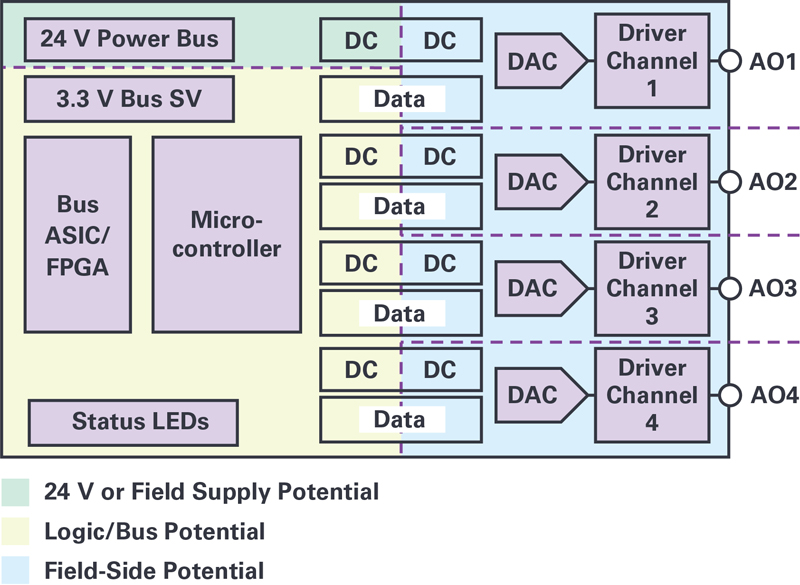
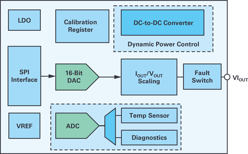
Figure 1. Block diagram of an isolated analog output system
Today’s typical programmable logic controller (PLC) contains a multitude of analog and digital inputs and outputs for the monitoring and control of industrial and production processes. Modularization is widespread and, with respect to inputs and outputs (I/Os), covers the basic functions of analog I/Os and digital I/Os. The analog output presents a particular challenge because, as shown in Figure 1, a set value must be driven actively and with high accuracy under numerous different load conditions. The active driver stage is important here; losses should be kept as small as possible.
The factors to be considered are as follows:
u Connected load
u Maximum allowable ambient and internal module temperatures
u Number of channels and size of the module
u Galvanically isolated interface
u Accuracy
In process automation, there is often an additional requirement for a galvanic barrier between individual output channels. Besides that, there are still other conditions such as channel-based diagnostics or support of HART signals. Robustness and fault tolerance are also prerequisites.
Thanks to developments in semiconductors and continuously improved mixed-signal processes, very small circuits with high integration densities are possible. The function of an analog output channel can be completely integrated in a single IC. Thus, within a 5 mm × 5 mm footprint, the AD5758 unites the basic function of a DAC and a driver plus numerous other analog and logic functions such as an ADC for diagnostics, intelligent power management, a voltage reference, a fault switch against reverse and overvoltages, a register for calibration data, and the SPI communication interface.
The AD5758 (Figure 2) covers all common output ranges used in the automation world: unipolar 0V to 10V/0mA to 20mA, bipolar ±10V/ ± 20mA, and all subranges such as the 4mA to 20mA used in process automation. Each setting offers a 20% overrange. The values are output with a 16-bit resolution.
Click image to enlarge
Figure 2. Block diagram of the AD5758
Power efficiency optimization
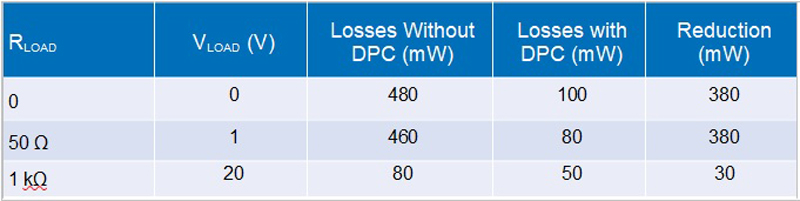
What makes the AD5758 particularly suitable for temperature- and space-critical applications? Losses, in the form of heat, occur mainly in the power section with the dc-to-dc converter and the output driver stage. This is where intelligent power management comes into play. The AD5758 features adaptive load regulation or dynamic power control (DPC). DPC is active during current output mode and controls the voltage in the driver stage needed to drive a specific current into a load. Depending on the operating condition, the load voltage for the current output (I × RLOAD) may only make up a fraction of the supply voltage. The difference with respect to the supply voltage must be dissipated in the series transistor in the form of a power loss, which generates heat. The DPC now regulates the driver voltage to a few volts above the actual required load voltage (headroom for output transistor) and thus provides for minimal thermal dissipation. Efficient adjustment of the voltage in this way is only possible via a buck switching regulator, which is already integrated in the AD5758 and is automatically controlled based on the load. Even if additional losses arise in the switching regulator and in the upstream power supply, the overall thermal reduction is very effective, especially for small load resistances; see Table 1. It makes smaller, higher density designs possible in the first place and the board stays cool.
Click image to enlarge
Table 1. Theoretical Losses for an Output Current I = 20 mA and a Fixed Supply Voltage of 24 V (Internal Power Consumption and Efficiency of DC-to-DC Not Taken into Account)
Derating sets tight limits
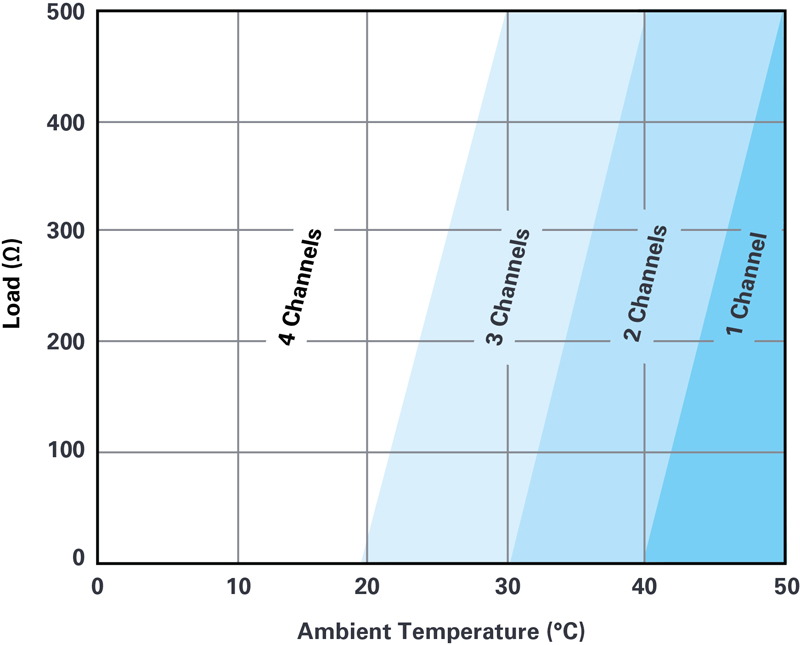
Derating is defined as a reduction in performance under defined boundary conditions, similar to the safe operating area (SOA) consideration in power semiconductors. Because of the previously mentioned power loss and associated cooling problems, tight thermal limits are imposed on those output modules without DPC. Today, two or four channels on a credit card-sized module are common. The modules are usually specified for ambient temperatures of up to 60°C. Under these environmental conditions, however, not all four channels can drive very small loads because without DPC, those four channels would generate power loss in the module of around 3 W and the heat generated can quickly raise the internal module temperature to beyond the max spec of the components. With thermal derating (Figure 3), the module manufacturer restricts the use to only one or two of the available four channels at high ambient temperatures, drastically worsening the usability and channel costs.
Click image to enlarge
Figure 3. Typical derating chart
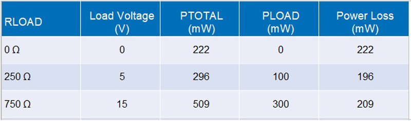
Thanks to its highly efficient DPC, the AD5758 has a power loss that only slightly depends on the load resistance and the total channel dissipation always remains at <250 mW for loads of 0 kΩ to 1 kΩ (Table 2). Thus, depending on the design of the output module, it may be possible for eight isolated channels to be realized at <2 W in the worst case. The 5 mm × 5 mm LFCSP with its thermal resistance from junction to ambient ΘJA of 46 K/W increases the ambient temperature by less than 10°C at a power loss of 200 mW. The AD5758 is specified for use in ambient temperatures of up to 115°C. This offers a lot of headroom for multichannel modules without the need for derating.
Click image to enlarge
Table 2. Measured Power Values in DPC Operation at I = 20 mA and Supply = 24 V
The power loss numbers are for the complete channel and also include the dissipation due to power and data isolation using the ADP1031.
Optimized power supply
The supply voltages have different requirements:
u Logic voltage: Apart from the (operating mode dependent unipolar or bipolar) driver supply, the AD5758 output IC requires a 3.3 V logic voltage for the internal blocks. This can be generated with the on-chip LDO regulator; however, for optimal efficiency and a lower power loss, a switching regulator is recommended.
u Isolated driver supply: For safety reasons, the PLC bus is always galvanically isolated from the I/O modules. Figure 1 shows this isolation with color coding for the three different potentials of logic (bus) side, voltage supply, and field-side output.
Because these three sections are also often spatially separated on the board—the outputs are positioned toward the front connector terminals, while the backplane bus is, as the name says, at the back—integration of the isolation, power supply, and output driver on a single chip would not make sense.
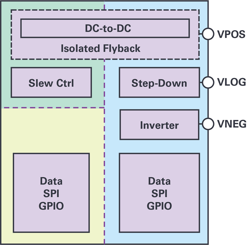
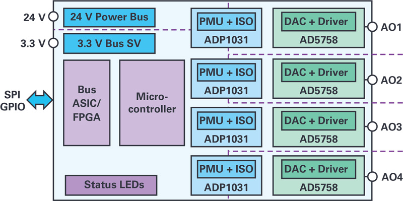
The power management unit ADP1031 (Figure 4) performs all functions and, together with the AD5758, enables development of isolated output modules with minimal space requirements and power loss (Figure 5).
The ADP1031 integrates four blocks on 9 mm × 7 mm package:
u Flyback converter for generation of an isolated positive supply voltage VPOS.
u Inverter for the negative supply for bipolar outputs VNEG.
u Step-down converter for supply of the AD5758 logic circuits with VLOG.
u Isolated SPI data interface with additional GPIO channels.
Click image to enlarge
Figure 4. Power management unit ADP1031
Click image to enlarge
Figure 5. Complete 4-channel analog output with the ADP1031 and AD5758
The advantage of the flyback converter is its high efficiency; only a small 1:1 transformer is needed. The flyback converter generates the isolated driver voltage of up to 28V in the first stage. The inverter and the step-down converter are derived from this and share the same ground potential.
During the design of the power management unit, special emphasis was placed on electromagnetic compatibility (EMC) and robustness. For example, the output voltages are phase-shifted and the slew rate of the flyback controller is adjustable. Soft start, overvoltage protection, and current limitation for all three voltages are also added for good measure.
The isolated SPI interface is based on ADI’s iCoupler technology and transfers all control signals required for operation. Distinction is thereby made between a high speed path (four channels) for the SPI data and a slower path (three channels multiplexed) for control of GPIO. Possible applications are synchronous activation of the outputs in multichannel modules or across several modules via a common control signal, reading-back an error flag, or triggering a safety shutdown.