ADI's RF Front-End Family Enables Compact 5G Massive MIMO Network Radios
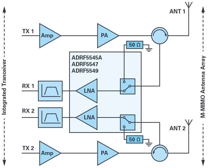
Figure 1: M-MIMO RF front-end block diagram
Massive multiple input, multiple output (M-MIMO) radios have seen their popularity surge in the late stage deployment of 4G LTE cellular base stations, particularly in dense urban areas where small cells effectively filled the cellular coverage voids while boosting higher data speed services. The success of this architecture clearly proved its worth. It is poised to be the architecture of choice for nascent 5G network radios, as required spectral efficiency and transmission reliability characteristics are inherent to this architecture. The challenge to making 5G a reality is that designers must vastly increase the number of simultaneous transceiver channels operating in multiple bands, while also squeezing all the necessary hardware into a form factor that is as large as or smaller than in the previous generation’s equipment.
The implications of doing so are:
- More channels means higher concentrated RF power in and around the base station, so the problem of isolation between channels without mutual interference is exacerbated.
- Receiver front-end components must have improved dynamic range performance in order to remain robust in the presence of high-power signals.
- Solution size matters.
- Thermal management must be addressed with the increased electronics’ and transmitters’ power.
In this quest for higher data rates to support a variety of wireless services and different transmission schemes, system designers face higher circuit complexity but must meet similar budgets for size, power, and cost. Adding more transceiver channels in a base station tower yields higher throughput, but utilizing each channel at a higher RF power level is equally essential for keeping system complexity and cost at acceptable levels. For higher RF power, hardware designers do not have many alternatives in their RF front-end design but to rely on legacy solutions that need high bias power and complex peripheral circuits, which makes achieving design goals more difficult.
Analog Devices recently introduced an integrated high-power switch with a low noise amplifier (LNA) in multichip modules for time division duplex (TDD) systems. The family covers cellular bands from 1.8GHz to 5.3GHz and it is optimally designed for M-MIMO antenna interfaces. Incorporating a high-power switch in silicon process and a high-performance low noise amplifier in GaAs process, this new family of devices offers high RF power handling capability together with high integration without any compromise—meaning it’s the best of both worlds.
Dual-Channel Architecture
An ADRF5545A/ADRF5547/ADRF5549 application block diagram for a M-MIMO RF front-end design is shown in Figure 1. The device has channels that incorporate a high-power switch followed by a two stage LNA. During receive mode operation of the transceiver, the switch routes the input signal to the LNA input. During transmit mode, the input is routed to a 50 Ω termination to ensure proper matching to the antenna interface and to isolate the LNA from any reflected power from the antenna. The integrated dual-channel architecture allows designers to easily scale their MIMO to exceed the legacy equipment’s limit of 8 × 8 (8 transmitter × 8 receiver) configurations —to 16×16, 32×32, 64×64, and beyond.
Wide Operation Bandwidth
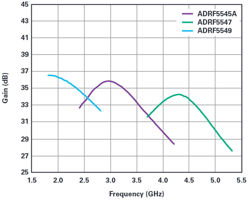
ADRF5545A/ADRF5547/ADRF5549 gain characteristics of each device and their respective frequency coverage is shown in Figure 2. Parts are optimized for commonly used cellular bands and aligned with other tuned components used in the same design, such as power amplifiers and filters.
Click image to enlarge
Figure 2: ADRF5545A/ADRF5547/ADRF5549 gain characteristics
High Power Protection Switch
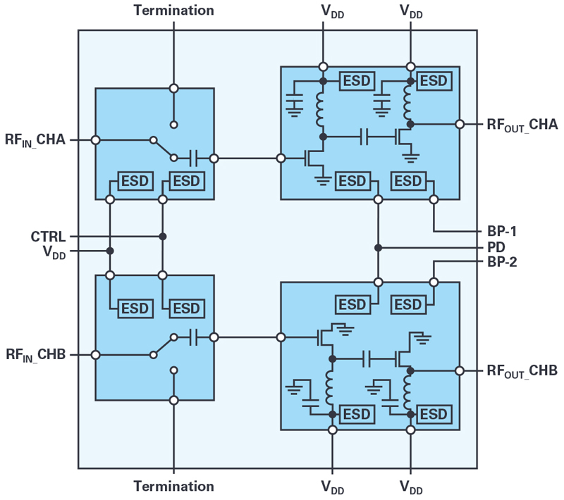
The device incorporates a high-power switch designed in silicon process that does not need any external components for bias generation. The switch runs on a single 5 V supply with only 10 mA current consumption and can interface to standard digital microcontrollers directly without need for any negative voltages or level shifters. Compared to an implementation using PIN diode-based switches, the silicon switch saves the user around 80% bias power and 90% circuit board area.
The switch can handle 10 W average RF signal with 9 dB peak-to-average ratio (PAR) in continuous operation and can withstand double the rated power in a fault condition. The ADRF5545A/ADRF5547/ADRF5549 are the first products in the market that feature 10 W power handling capability, which makes them ideal for high power M-MIMO designs. If more power can be transmitted from each antenna element, the number of transmit channels can be reduced to get the same RF power out of the base station. The ADRF5545A/ADRF5547/ADRF5549 architecture is shown in Figure 3, which reveals that the high power switch for both channels are supplied and controlled on the same device pin. The LNAs have their supplies and control signal separate.
Click image to enlarge
Figure 3: ADRF5545A/ADRF5547/ADRF5549 circuit architecture
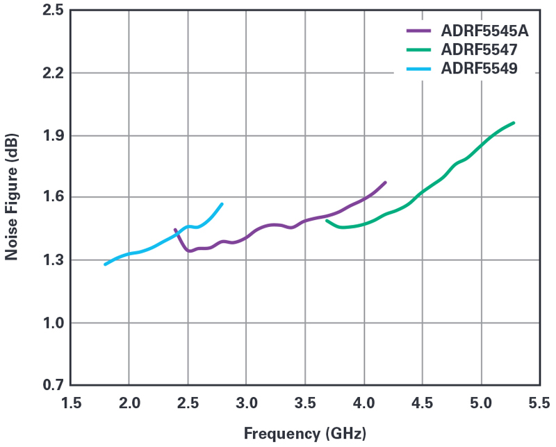
Low Noise Figure
A two stage LNA is designed in GaAs process, supplied by a single 5 V supply, and does not need any external bias-tee inductors. The gain has flat characteristics over frequency and is programmable to 32dB and 16dB in high and low gain modes, respectively. The device also features a low power mode to save bias power where the LNAs can be powered down during transmit operation. The device has a noise figure of 1.45 dB including the insertion loss of the switch, which is well suited both for high power and lower power M-MIMO systems. Figure 4 shows the noise figure performance of the ADRF5545A/ADRF5547/ADRF5549 in specified bands.
Click image to enlarge
Figure 4: ADRF5545A/ADRF5547/ADRF5549 noise figure
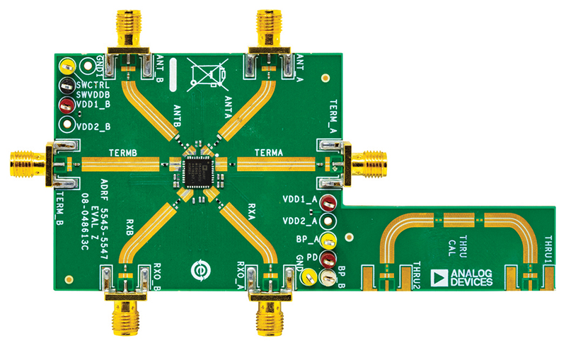
Compact Size, Minimum Set of External Components
Besides the primary decoupling capacitors on supply pins and dc blocking capacitors on the RF signal pins, the device does not need any tuning or matching components. The RF input and outputs are 50Ω matched. The LNA has the matching and bias inductors integrated in the design. This reduces the bill of material for expensive components such as inductors but also simplifies the hardware design for channel-to-channel crosstalk between adjacent transceivers. The device comes in a 6mm×6mm surface-mountable package with a thermally enhanced bottom paddle. The device is specified to operate at case temperature in the range from –40°C up to +105°C. All three parts are assembled in the same package and have the same pinout. They can be used interchangeably on the same circuit board. The device is shown as mounted on its evaluation board in Figure 5. Evaluation boards are available from ADI directly or through its distributors.
Click image to enlarge
Figure 5: ADRF5545A/ADRF5547/ADRF5549 evaluation board