Advanced design topics for off-line flyback power supplies – Part 1
Using an on-line design tool can help your efforts
The flyback is the simplest and most commonly used isolated power-converter topology, able to step voltage up or down while providing galvanic isolation from the ac mains in off-line applications. It is the most cost-effective topology for powering many kinds of electronic equipment, having acceptable efficiency and small enough size as long as the output power is less than about 200W. We will cover some of the finer points of designing flyback converters, and an on-line expert system called Power Supply WebDesigner (PSW).
A standard flyback converter takes ac or dc input and one secondary-side-regulated output, plus up to two additional cross-regulated outputs. The design includes a wire-wound transformer, an RCD clamp (sometimes called a snubber) on the primary side, and one or two stages of filtering on each output. An important part of the design is the selection the right controller+MOSFET, because the design must be tailored to the built-in limits of this component. These controllers have external control-loop compensation, which is also addressed here.
While the standard flyback converter is most common, there are other more complex variations not covered here that are designed to meet specific needs. For example, a two-switch version reduces the voltage rating of the main switch but adds a second power switch and a high-side drive. An active-clamp version increases efficiency and further limits voltage stress on the main switch but adds an auxiliary switch. A final example is quasi-resonant operation, which reduces turn-on losses but increases control complexity and limits operation to boundary- or discontinuous-conduction mode.
Our main purpose is to explain how to make the design choices necessary for a flyback converter, whether using PSW or any other design method. PSW will make all these choices automatically, but it offers great flexibility in allowing the user to change any of them and see the effects in a matter of seconds. For this reason it’s also an excellent tool for learning about flyback design, and most of the guidance offered in this paper is included in “information notes” available at appropriate places throughout the design procedure. As a result, there should be no need to refer to other documentation to complete a flyback design, but if more detail is desired, a complete design procedure and many of the embedded design equations are provided in an application note. Other application notes address more specific aspects of flyback design, including the use of synchronous rectification at the output.
Flyback Converter
The standard flyback converter as shown in Figure 1 is widely used in low-power (<200W) and/or high-voltage applications due to its low part count and ability to deliver multiple outputs with few additional parts, although cross-regulation is inferior to isolated buck-derived converters. The converter is often operated in discontinuous conduction mode (DCM), especially at less than 50W, where the magnetizing current returns to zero at the end of each switching cycle and may remain there for some time, until the start of the next switching cycle. The control design is very simple for DCM, described by the same equations as a non-isolated buck-boost topology but with a turns ratio inserted.
Click image to enlarge
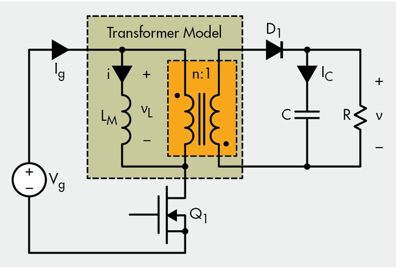
Fig. 1. Power train of a flyback converter where the transformer is represented by a model consisting of an ideal transformer plus magnetizing inductance.
The “transformer” of a flyback converter is actually used as a coupled inductor, where the primary winding conducts current during a different portion of the switching cycle than the secondary winding(s). As a result, all the energy transferred from the input to the output must be alternately stored and discharged from the magnetizing inductance, which requires a small magnetizing inductance relative to most isolated topologies. While the instantaneous winding voltages are related by the turns ratio, the instantaneous and rms winding currents are not. Basic waveforms of the converter operating in continuous- and discontinuous conduction mode are shown in Figure 2.
Click image to enlarge
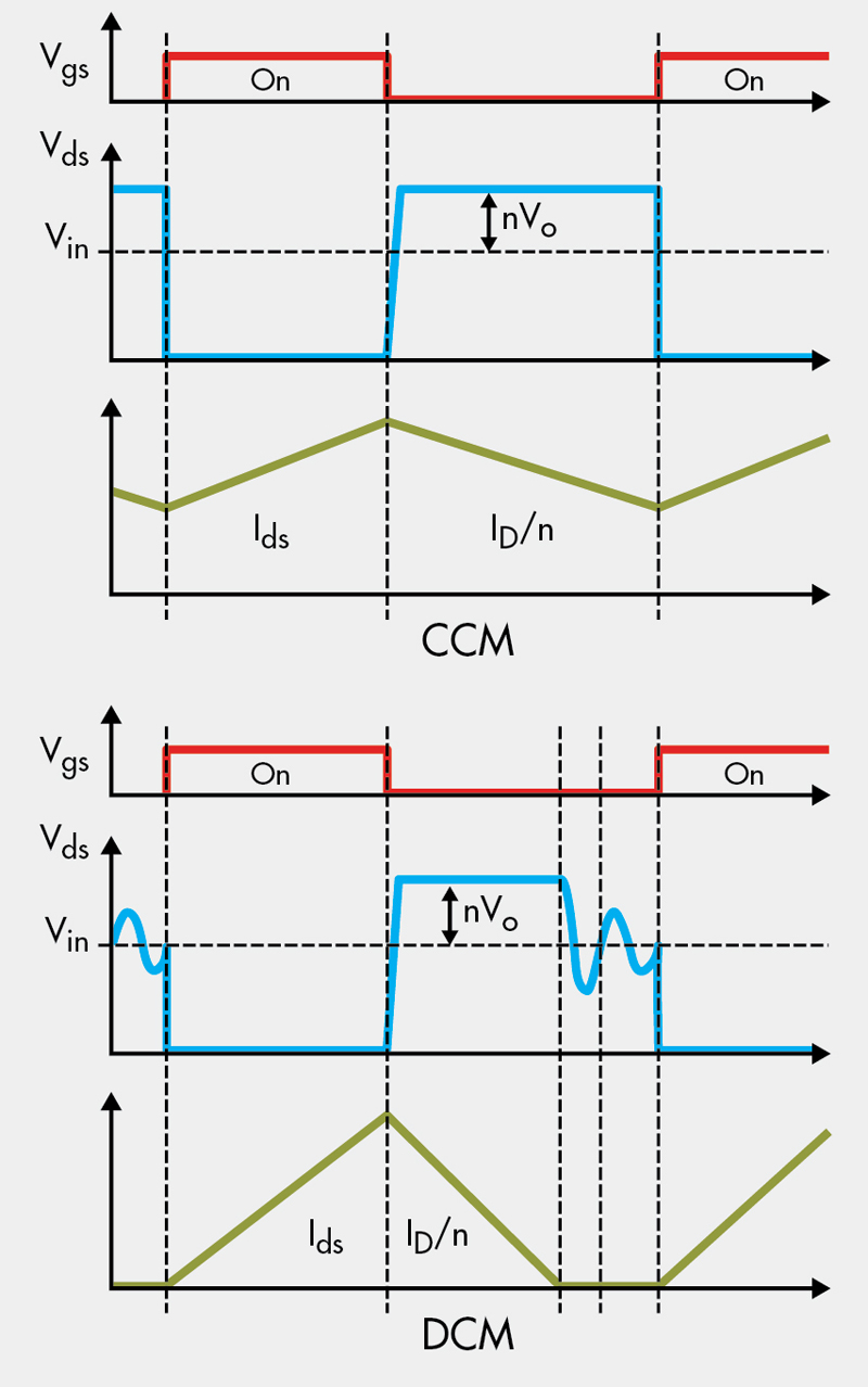
Fig. 2. Basic waveforms of a flyback converter operating in continuous conduction mode (CCM) and discontinuous conduction mode (DCM), where the lower waveform in each set is the transformer magnetizing current.
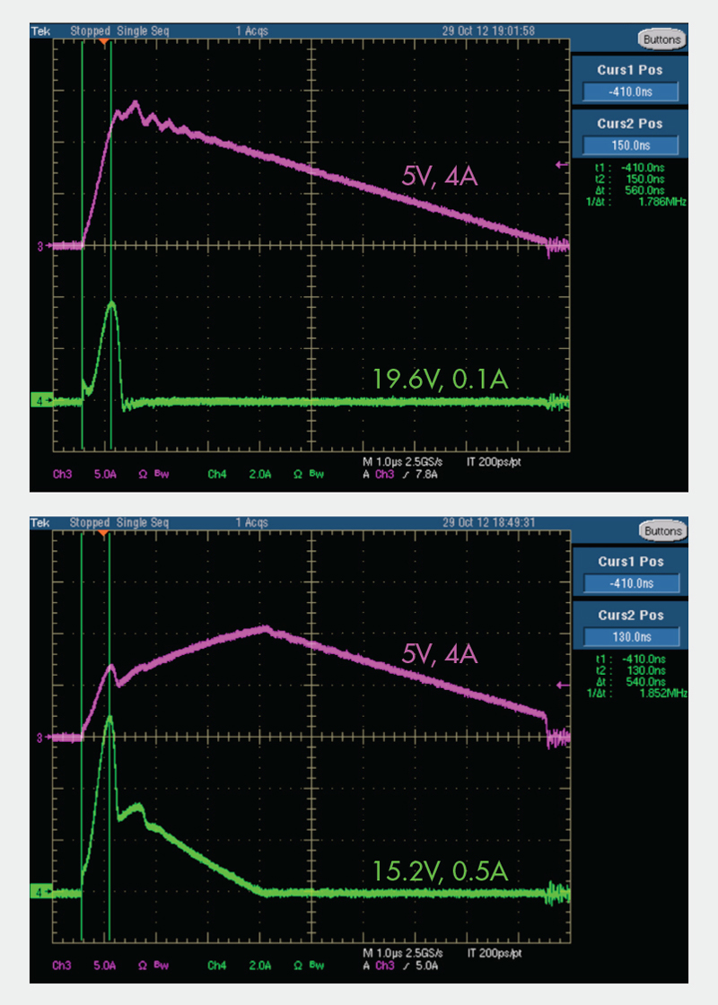
For a multiple-output flyback converter, Figure 3 illustrates two important points. One is the output-diode conduction times for different outputs can be different, and it depends on the relative loading. In fact, the lower set of waveforms shows output 2 in DCM while output 1 operates in CCM, evidenced by the abrupt step of current down to zero at the end of the conduction time. The second point is that cross-regulation becomes poor at very light load, evidenced by output 2 rising from 15.2V at 0.5A load to 19.6V at 0.1A---and 31.5V at no load! (Not shown.) To protect the loads on cross-regulated outputs, often a minimum load is specified or zener-diode voltage clamps are installed across those outputs.
Click image to enlarge
Fig. 3. Waveforms of output-diode current for output 1 (magenta) and output 2 (green) for two different loads on output 2.
Power Supply WebDesigner
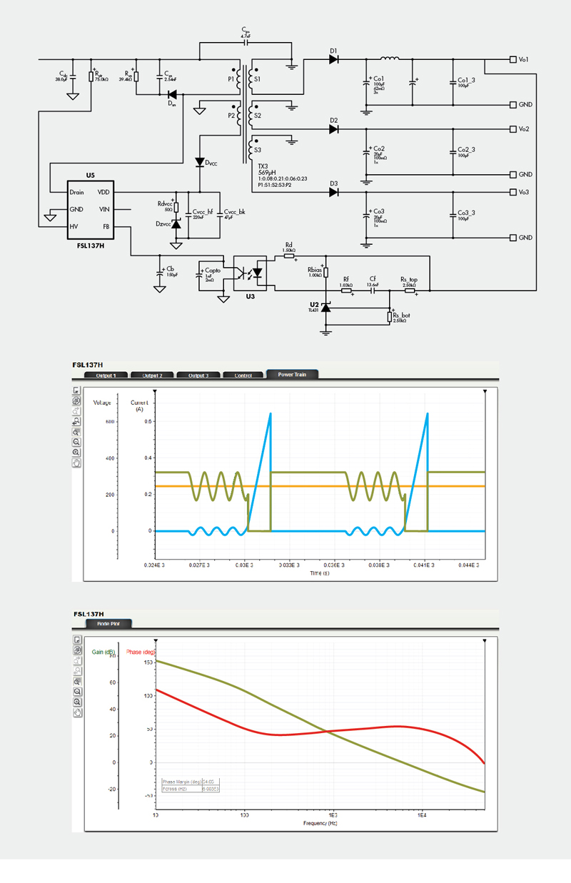
On Fairchild Semiconductor’s website is a sophisticated, web-based design and simulation tool called Power Supply WebDesigner (PSW), with example output shown in Figure 4 and other figures of this paper. It’s “auto design” feature classifies it as an expert system, able to make the numerous design choices explained in the next section without user intervention, based on the experience of expert designers captured in its algorithms. If a user would like to make adjustments to the design, he/she can review the detailed design procedure and override the “recommended” value of any design variable, guided by text information notes and dynamic limits that ensure input is reasonable. After manual adjustments are made, the tool recalculates later recommended values to optimize the design given the new input. A user may then continue stepping through and reviewing each design step, or at any time he/she may have the tool complete the rest of the design automatically.
Click image to enlarge
Fig. 4. Examples of some output from Power Supply WebDesigner™ (PSW): design schematic, waveforms, and Bode plot.
PSW generates a complete, prototype-ready schematic with all the necessary components, and it provides results from four types of circuit analysis: calculated component losses, steady-state waveforms, transient waveforms, and loop-gain Bode plots to indicate stability. (Only component losses and Bode plots are included in this paper, to illustrate the effects of some manual design changes.) If any results are unacceptable, further adjustments can be made in the design procedure (with the benefit of error and limit checking), or component values can be changed directly on the schematic diagram. Finally, a bill of materials is generated with the option to choose parts and assemble an order from catalog distributors of electronic components.
Although not covered in this paper, the SIMPLIS™ piecewise linear circuit simulator is used to provide simulation and stability results on-line, using circuit models that have been simplified sufficiently to provide results in less than one minute. As a result, it cannot predict higher order-effects such as voltage ringing; therefore simulated waveforms won’t look like lab measurements. The simulation also cannot predict detailed component-level behavior or losses, power factor, THD or EMI. Nevertheless, the model CAN predict steady-state, ac (stability) & transient behavior; it can confirm proper design margins at corner cases of operating conditions. These simplified simulation models have been validated against more sophisticated models (which take longer to run) as well as lab measurements made on selected test circuits.
In Part II, we will continue our discussion, starting with Basic Design Choices.
WEB ONLY
REFERENCES
[1] Power Suppy WebDesigner, an on-line design tool from Fairchild Semiconductor. Available: www.fairchildsemi.com/psw
[2] “Integrated Critical-Mode PFC/Quasi-Resonant Current-Mode PWM Controller FAN6920),” Fairchild Semiconductor Application Note AN6920-MR, Rev. 1.0.0, 2013. Available: www.fairchildsemi.com/an/AN/AN-6920MR.pdf
[3] Robert Watson III, “New Techniques in the Design of Distributed Power Systems,” Ph.D. dissertation, Dept. of Elect. and Computer Eng., Virginia Polytechnic Institute and State Univ., Blacksburg, VA, 1998. Available: http://scholar.lib.vt.edu/theses/available/etd-71398-22552/
[4] “Design Guidelines for Flyback Converters Using FSQ-series Fairchild Power Switch (FPS™),” Fairchild Semiconductor Application Note AN4150, Rev. 1.0.0, 2006. Available: www.fairchildsemi.com/an/AN/AN-4150.pdf
[5] “Design Guidelines for Off-line Flyback Converters Using Fairchild Power Switch (FPS),” Fairchild Semiconductor Application Note AN4137, Rev. 1.2.0, 2003. Available: www.fairchildsemi.com/an/AN/AN-4137.pdf
[6] “Transformer Design Consideration for Offline Flyback Converters Using Fairchild Power Switch (FPS™),” AN-4140, Rev. 1.0.0, 2003. Available: www.fairchildsemi.com/an/AN/AN-4140.pdf
[7] “Design Guidelines for RCD Snubber of Flyback Converters,” AN-4147, Rev. 1.1.0, 2006. Available: www.fairchildsemi.com/an/AN/AN-4147.pdf
[8] “Audible Noise Reduction Techniques for FPS ,” AN4148, Rev. 1.0.0, 2005. Available: www.fairchildsemi.com/an/AN/AN-4148.pdf
[9] “Troubleshooting and Design Tips for Fairchild Power Switch (FPS™) Flyback Applications,” AN4141, Rev. 1.0.0, 2003. Available: www.fairchildsemi.com/an/AN/AN-4141.pdf
[10] “Applying FAN6224 [Synchronous-Rectifier Controller] for Flyback and Forward Freewheeling Rectification,” AN-6224, Rev. 1.0.1, 2013. Available: www.fairchildsemi.com/an/AN/AN-6224.pdf
[11] Robert W. Erickson and Dragan Maksimovic, “Fundamentals of Power Electronics,” Second edition, Kluwer Academic Publishers, 2001, ISBN 0-7923-7270-0.