The battle raging to raise power supply density with ever more efficiency
The battle raging to raise power supply density with ever more efficiency
By The battle raging to raise power supply density with ever more efficiency
Considering practical design limitations, some smart developments are shifting the focus over the next few years from ‘just’ power conversion to ‘perfect’ power conversion for POL regulation. Skyrocketing demand for data-centric services, including consumer video streaming, is placing an increasing burden on infrastructure capacity and speed with a knock on effect on the electronic industry as a whole. This is the cycle that fuels innovation, driving to increase processing speed and data throughput. Annually, IC companies deliver faster processors by squeezing more from Moore’s law. All the while, there’s a battle raging to raise power supply density whilst eking out ever more efficiency.
In the last decade alone, the supply voltage for high-density logic and processor devices has fallen from an average of 3V, to as low as a 0.6V threshold level in some cases. Similarly, power demands for server-class equipment, which are generally thermally limited, are still up to and beyond 100W. The result is a current demand approaching a 100A threshold at the point of load (POL) with increasingly tight voltage tolerances. This is a shift stressing conventional power conversion architectures and circuit design. It’s demanding a revolution in the way system suppliers and component manufacturers deal with the emerging compromises forced into the design mix.
Why Point of Load?
The use of point of load power conversion has been on the rise for many years now. And, with higher and higher POL currents, it makes sense to distribute a single power rail throughout a system and then locally converting it to meet other voltage requirements. The benefits of this approach are already well understood and includes: ease of distribution and routing in complex rack systems, thermal (heat) distribution limiting hot-spot formation, optimal voltage regulation and system modularity facilitating functional hot-swapping.
Distributed power architectures for processor-intense systems have relied on an intermediate DC power bus at 12 V, then generating the system voltages locally, at point of need. System voltages range from sub 1V requirements for processor cores to 2 to 5V in support of peripheral components. Though this trend continues un-abated, local power needs are reaching a point where certain physical constraints are forcing a re-think. The dominant issue is the ever-decreasing processor core voltage. The rationale driving this decrease is the greater share that dynamic power consumption contributes to the total system power budget today. Dynamic power consumed by a processor is proportional to its clock frequency and the square of its supply voltage. Thus, the trend towards lower core voltages is obvious (especially at high clock rates).
Worse still, from an implementation perspective, as core voltages drop, the provision of voltage regulation is increasingly tougher. Several issues can be identified: the delivery of tight tolerance regulation necessitates a reduction of PCB trace lengths to reduce voltage drops. This in turn creates size reduction pressures on energy storage components, in turn promoting increased switching frequency.
“Bucking” the trend
Any changes in the power management implementation must focus on further efficiency improvements with a drive towards perfection (>95%). To date, the workhorse architecture for distributed power has been the synchronous buck convertor. Its attractive features include: relative circuit simplicity, high efficiency (>85%) and low cost.
However, two design aspects impact on the synchronous buck convertor’s merits. The first is that it is designed to ensure that the power switching devices remain in continuous conduction mode. This helps to ensure full load efficiency, but comes with the penalty of increased low load inefficiency.
Secondly, and perhaps more importantly, to achieve compact POL conversion, increases in switch frequency are desirable. Higher frequency switching translates into less energy transfer per cycle, helping reduce the physical dimensions of the energy transfer components (i.e. the inductor and capacitors). However, as the output to input voltage ratio falls, the on time for the synchronous buck rapidly shrinks - raising power loss. So the synchronous buck’s deficiency is made more apparent with falling core voltage.
Comparing electrical conversion in the Buck and SEPIC-fed buck (SFB)
In a standard buck, the switching duty cycle (DB) is dependent on the ratio of output to input voltage (DB = EOUT/EIN). So for a 12V step down to 1.2V, DB = 0.1 – i.e. the switch is on for 10% of the switching cycle. In this case, as core voltage falls the switching time of the power device is compressed. As DB falls, the power switch operates increasingly more within its dynamic switching zone (linear) and thus energy losses accumulate rapidly impacting efficiency.
Now consider the SFB. The duty cycle (DSFB) is defined slightly differently as (DSFB = (2 x EOUT)/(EIN + EOUT) ). In this case the duty cycle of the SFB with a 12V rail and 1.2 V output is given as: [DSFB= 2 x 1.2/(12+1.2) = 2.4/13.2 = 0.181]. That means switch on time has now almost doubled (18% versus 10%). This is a really useful property, especially when output voltage is small compared to input levels and when switch frequencies need to be increased to improve power density.
Another advantage of the SFB topology is that energy to the load is maintained by the SEPIC stage even when the buck circuit portion is ‘OFF’. This results in almost halving the peak circuit currents which need to be switched, lowering device stress. Furthermore, this factor helps increase power density, since smaller components can be specified with the inherently lower peak current handling requirement of this topology.
The benefits of the SEPIC-fed buck (SFB) architecture
The Solus(R) Power Topology recently developed by CUI Inc., comprising a SFB topology, represents a highly optimised solution to POL power provisioning. At its heart is just one magnetic component, a control switch and a pair of commutation switches that are precision controlled by a pulse-width modulated (PWM) signal provided by a switching regulator. The magnetic component is a compound device made from four inductively-coupled coils wound on one core. This slightly more complicated magnetic design still yields a relatively simple implementation not dissimilar to the standard buck architecture, helping to control costs.
The design focus for this innovative architecture has been to simultaneously improve efficiency and regulation. Increased efficiency comes from reducing both the conduction and switching losses at several critical circuit nodes within the topology. Better still, at increased switching frequencies, these improvements become more compelling. In fact, with identical switching devices deployed in a conventional buck and a Solus design, the new SFB topology has demonstrated the potential to reduce switching losses by over 90%, setting a new power density benchmark.
An example of what’s possible
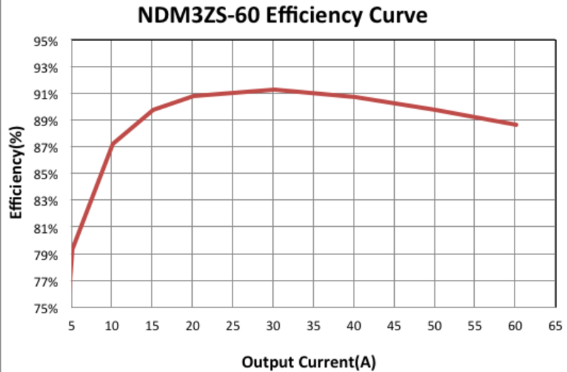
Using the Solus Topology, CUI has created the highly compact, non-isolated 60A NDM3ZS-60 module (see Figure 1). It operates from a 7.2 to 14 V input and can be programmed to provide an output between 0.6 to 1.5V. The efficiency of the module and its impressive transient load performance are shown respectively in Figures 2 and 3. The module design succeeds in lowering component voltage and current stresses. Coupled with an ability to exploit an inherent gate charge extraction process, the topology reduces switch turn-on losses by 75% and switch turn-off losses by 99% when compared to conventional buck converters. This translates to a peak efficiency of 91.1% at 12Vdc in to 1.0Vdc out, 50% load. Efficiency remains high up to full load at 88.9%.
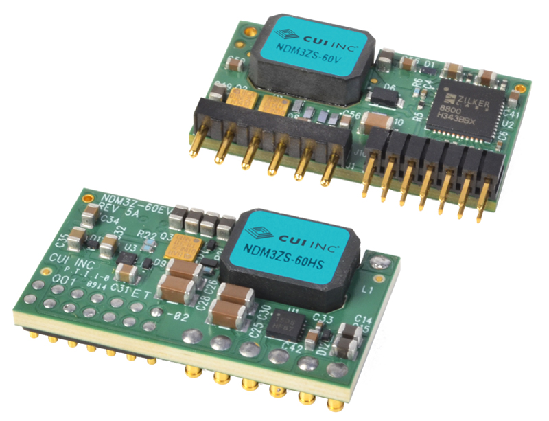
Click image to enlarge
Figure 1: CUI Inc.’s NDM3ZS-60 module.
Click image to enlarge
Figure 2: Efficiency curve for the NDM3ZS-60 module.
![]()
Click image to enlarge
Figure 3: Transient response (approx. 15mV) for a 10A output current step (lower trace).
It is worth noting the relative transient response performance benefit of the SFB topology when applied in the 60A module described here. At 12Vdc in to 1Vdc out with a 30A load step (from 15A to 45A) and a 10A/µs slew rate, peak voltage is under 10mV, staying within the critical 1% for many applications, with typical external capacitance required. The external capacitance required is one-third of other competing solutions, reducing cost and total solution board space.
A word on compensation – the evolution to digital
In a 2012 article , CUI discussed the evolution of loop compensation techniques for POL voltage regulation. Feedback is deployed to ensure stable operation of POL regulators in the face of varying system conditions such as: output loading, input disturbances, temperature and component aging effects. The loop compensation task falls on the switching controller IC. Originally, compensation was the domain of analogue experts. More recently though, digital controllers of increasing sophistication have emerged allowing compensation to become semi-automatic and more of an issue of moderate system tuning, often with the aid of an easy to use graphic user interface or GUI.
For its latest digital POL modules, CUI chose the 4th generation digital power controller from Intersil. The ZL8800 features dual PWM output channels, each capable of switching at up to 1.3MHz. A key feature is the proprietary automatic control system known as ChargeModeTM control. This uses a high-speed loop that allows the precise replenishment of charge lost from the output capacitor during a transient event. Control is performed rapidly, cycle-by-cycle as the digital loop over-samples the output voltage. Ingeniously, the ZL8800 does not need to know actual external component values, rather it relies on digital algorithms and multi-rate modulation to make its adjustments.
The end result is a reduction in the amount of bulk capacitance necessary for a given application yet the ZL8800 achieves excess bandwidth for enhanced load regulation. Finally, through inherent loop stability, the controller handles component tolerances as well as aging and environmental effects.
That’s two technical revolutions contained in one compact design; teaming an optimal topology (SFB) for low output voltage regulation with a leading edge digital controller for maximum power density, efficiency and ease of use. It’s a powerful combination of capabilities designed to address the growing need for perfect power conversion, under all conditions, all of the time.