Author:
Anjum Jabeen, Taku Takaku, and Yasuyuki Kobayashi, Fuji Electric
Date
09/29/2016
 PDF
PDF
Energy conservation and reduction in CO2-emissions are key factors in mitigating global warming and preserving our future environment. These positive trends are leading to wider usage of power semiconductors in energy conversion systems supplying the rapidly growing global energy demand. IGBT (Insulated Gate Bipolar Transistor) modules are the most common power semiconductors devices used in industrial, consumer, automotive, and renewable energy systems.
Since their introduction and commercialization in the power electronics market IGBT modules have seen a number of significant technological innovations contributing to the miniaturization and cost reduction of energy conversion systems. The miniaturization of the IGBT chip and the corresponding increasing power densities lead to an increase in chip temperature and, if unaddressed, will contribute to device degradation and impact the IGBT long-term reliability. Thus in order to realize the improvements in the IGBT chip characteristics there must be corresponding improvements in the thermal performance properties of the IGBT package to adequately address potential latent reliability issues.
For example, through the application of new and innovative technologies significant improvements in heat dissipation properties of Fuji’s 7th Generation X-Series IGBT modules have been achieved and serve to ensure sustained high temperature performance without compromising long-term IGBT module reliability. The improved performance of the 7th Generation X-Series IGBT module development was achieved through the simultaneous improvements of the IGBT chips and the module package. The 7th generation IGBT module with a high compactness and high power density creates the capability to work in a 175°C operating temperature condition and enables higher output currents compared to the previous generations of IGBT modules which are limited to a 150°C operating temperature condition.
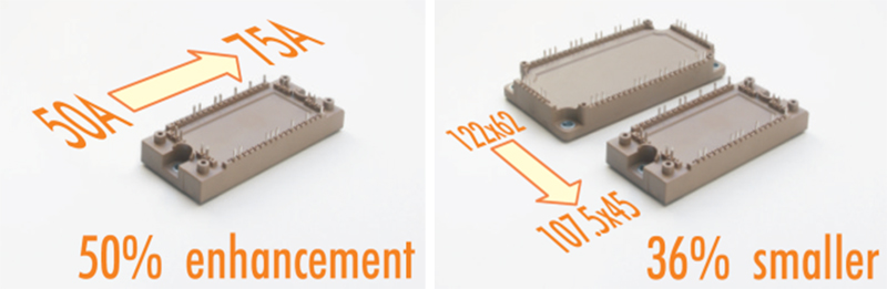
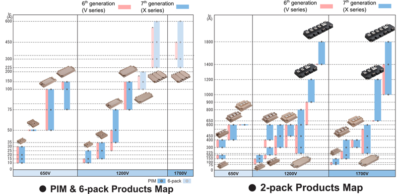
Figure 1 shows a comparison of current density and footprint size between 7th generation X-Series and 6th generation V-series IGBT module. The 1200V EP2 package (107.5mm x 45mm) was expanded up to 75A from the conventional 50A; a 50% enhancement. Additionally, the EP3 footprint size (122mm x 62mm) is reduced by 36% to the EP2 package (107.5 x 45mm). Furthermore, 7th generation IGBT achieves higher efficiency, continuous operation at Tj=175°C and improved ΔTj power cycling capability. Details of the new technologies for the 7th generation IGBT modules are described in this paper.
Click image to enlarge
Figure 1: Increased current density and downsizing of 7th generation X-series IGBT module
The 7th Generation Chip Technologies for 1200V
The 7th generation IGBT and diode characteristics have been improved and at the same time die size reduced and achieve higher efficiency. These innovative technology improvements are leading to a new generation of highly compact and efficient power conversion systems.
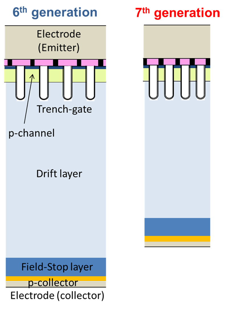
The cross-section of the 7th generation IGBT is shown in Figure 2. In the surface of the 7th generation IGBT chip the trench-gate structure was applied similar to the 6th generation IGBT. On the backside of the chip a Field-Stop (FS) layer was adopted on a thin FS-IGBT wafer. The drift layer thickness of the 7th generation IGBT was reduced by applying a thinner wafer compared to the 6th generation. As a result, the trade-off relationship between on-state voltage drop and turn-off losses was further improved by optimization of the surface structure.
Click image to enlarge
Figure 2: Cross-section diagram of the 6th generation IGBT (left) and the 7th generation IGBT (right)
The output characteristic of the 7th generation IGBT is shown in Figure 3. The on-state voltage drop of the 7th generation IGBT was reduced by 0.25V compared to the 6th generation at the same current rating by a thinner drift layer and an optimized surface structure (Tj=150°C) despite the reduced chip size.
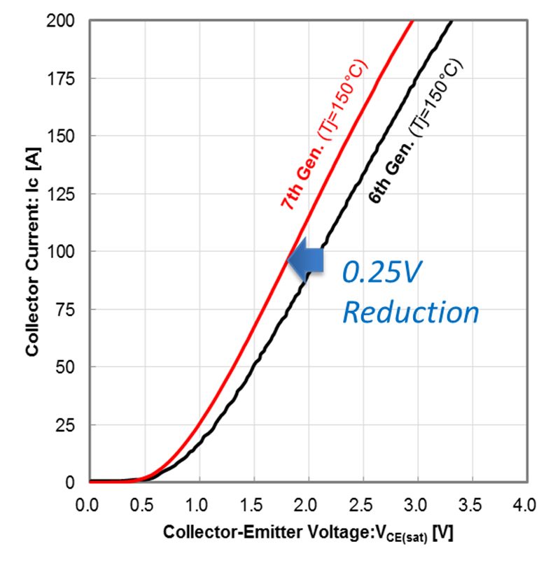
Click image to enlarge
Figure 3: Output characteristics of 7th gen. IGBT and 6th gen. IGBT. Tj=150°C, 175°C (7th gen.), VGE=+15V
The 7th generation IGBT´s turn-off losses were reduced by 10% compared to the 6th generation. This turn-off loss reduction was realized by the thinner drift layer applied as well as by the enhanced IE effect and the reduction of the Miller capacitance. The trade-off relationship between on-state voltage drop and turn-off losses is shown in Figure 4. On-state voltage drop was reduced by 0.25V from the 6th generation IGBT at the same current rating chip.
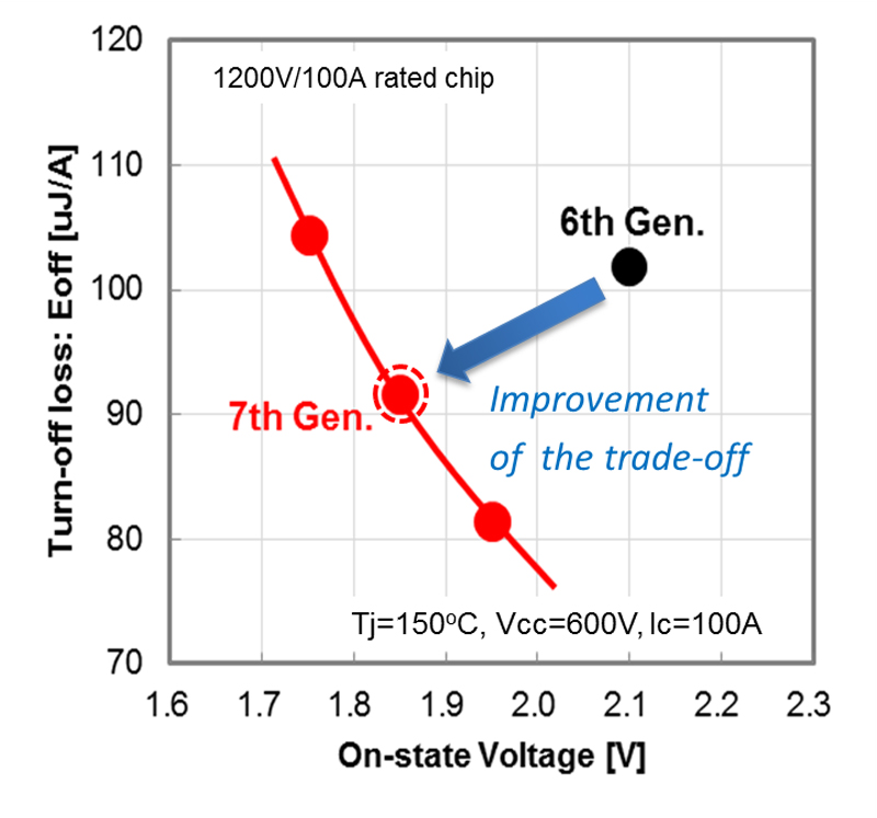
Click image to enlarge
Figure 4: Trade-off relationship between turn-off loss and on-state voltage drop. Tj=150°C, VCC=600V, VGE=+15V/-15V
The Diode Chip
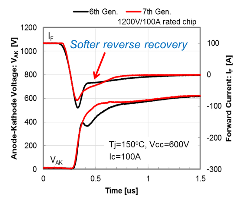
Compared to the 6th generation diode, the 7th generation forward voltage was reduced by 0.15V at the same current density (Tj=150°C). Figure 5 shows an example of reverse recovery switching waveform of the 7th generation diode. Compared to the 6th generation diode, the 7th generation diode realizes a much softer switching waveform by optimization of the local lifetime control. This softer switching waveform contributed to 21% reduction of the reverse recovery peak current and finally to a reverse recovery loss (Err) reduction of 15%.
Click image to enlarge
Figure 5: Reverse recovery switching waveforms of 7th generation diode and 6th generation diode. Switching conditions: Tj=150°C, VCC=600V, IC=100A (1x Inom), VGE=+15V/-15V.
The forward voltage of the 7th generation diode was reduced by reduction of the drift layer thickness. In recent years the requirements for IGBTs are not only loss reduction but also low EMI (Electro-Magnetic Interference) noise. EMI noise is known to be strongly related to the voltage changing during switching (dv/dt), in order to suppress EMI noise, it is necessary to reduce the dv/dt at low reverse recovery current which is the steepest dv/dt.
However, in order to reduce the dv/dt of the reverse recovery, it is necessary to slow down the switching speed with larger gate resistance, which will at the same time lead to an increase of turn-on loss (Eon). By improving the trade-off between the dv/dt and the switching losses, both low EMI noise and highly efficient power conversion systems can be achieved. The trade-off was improved compared to the 6th generation due to the reduction of the dv/dt by softening the reverse recovery current.
The 7th Generation Package Technologies
Size reductions of the IGBT and diode chips are required in order to achieve a higher current density of the IGBT modules. Actual result of the chip shrinking is an elevated power density within the modules which leads to increasing junction temperatures and related degradation of the reliability. For the 7th generation the packaging technologies were further improved developing a reliable, highly heat dissipating, and, heat resistant package. The new package realized not only the suppression of rising junction temperatures, but also enables 175°C operating temperature at the same high reliability level.
Improvement of ΔTj Power Cycling Capability
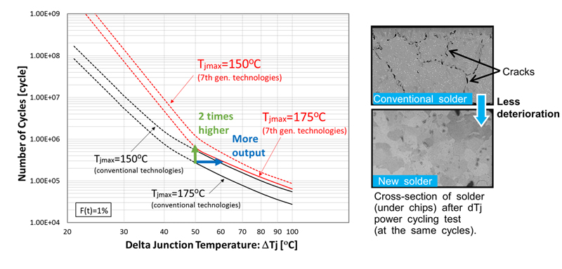
In order to achieve a long lifetime for power conversion systems, a long-term high reliability IGBT module is necessary. In particular, the power cycling capability against repeating thermal stress is very important. The 7th generation IGBT modules expands the operation temperature up to 175°C which enables working with higher output currents compared to previous generations. Generally, the higher junction temperature reduces the delta Tj power cycling capability by the accelerated degradation of materials around chip. In delta Tj power cycling mode, the wire bonding contacts on the chip and the solder under the chip are facing the greatest thermal stress so they are the first to start deterioration.
In the 7th generation IGBT modules, wire diameter and length were optimized and a newly developed high strength solder material was applied which significantly improved the delta Tj power cycling capability. As shown in Figure 6, by applying these new technologies, the 7th generation IGBT modules achieves 2 times the capability against conventional technologies at Tjmax=175°C. As a result, even if the modules are operating at Tj=175°C the highly improved power cycling capability enable them to achieve equal or even better long-term reliability.
Click image to enlarge
Figure 6: ΔTj power cycling capability curve
New High-Heat-Resistant Silicone Gel
In order to ensure the long-term reliability of the new IGBT modules the deterioration of the silicone gel at higher operating temperatures was the next challenge. Generally higher temperatures are hardening the silicone gels and cracks start occurring. These cracks will lower the isolating capabilities of the silicone gel. Therefore, a new highly heat resistant silicone gel was developed which allowed continuous operation at a temperature of 175°C.
The lifetime of new silicone gel at 175°C was further improved compared to current silicone gel, and same lifetime of current silicone gel at 150°C was realized. The new silicone gel simultaneously improves the hardening at low temperatures thus a long-term insulating capability at low temperature is realized.
Increasing Current Density of IGBT Modules
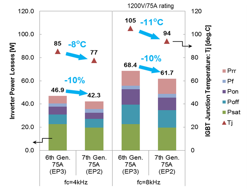
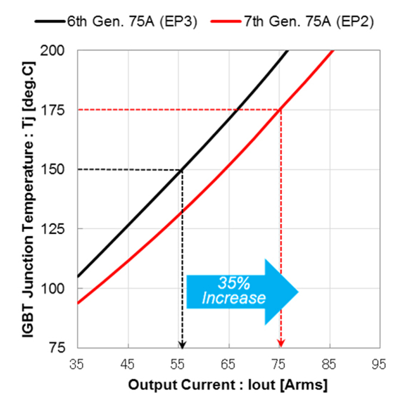
By further improvement of the losses of the 7th generation IGBT and diode and by additional improvement of the heat dissipation performance, an enhanced power density could be achieved. For example, compared to the 6th generation, the 7th generation reduces inverter power losses by 10% and IGBT junction temperature by 11°C (switching frequency fc = 8kHz) as shown in Figure 7. The maximum current rating of 1200V IGBT module in EP2 package (footprint size: 107.5mm x 45mm) is 50A by using 6th generation technologies. By applying the 7th generation chips and improved package technologies, a maximum rated current of 75A can be achieved as shown in Figure 8.
Click image to enlarge
Figure 7: Comparison of Inverter loss and IGBT junction temperature between the 7th gen. EP2 (75A rated) and the 6th gen. EP3 (75A rated). Conditions: VDC=600V, IO=35Arms, fO=50Hz, dv/dt=10kV/μs, Ta=40°C, Rth(f-a)/leg=0.60°C/W
As the result, the rated current of the 1200V EP2 package was expanded to up to 75A from conventional 50A and the footprint size could be reduced by 36% against the EP3 module.
7th generation IGBT modules offer two directions, which are a smaller footprint providing same output current as previous generations with higher power cycling capability or increasing the output current with the same footprint up to 35% as shown in Figure 8.
Click image to enlarge
Figure 8: Comparison of output current dependence of IGBT junction temperature (fc=8kHz)
7th Generation Module Line-Up Plan
As a result of the increased current density, Fuji Electric will be able to offer the 7th generation (X-series) IGBT modules with higher nominal current capability at the same footprint size. Please see the modules overview in Table 1. This product range is the first step of the product development with our new 7th generation of silicon chips. Additional module types are under consideration for future development.
Click image to enlarge
Table 1: Module line-up for 650V, 1200V and 1700V 7th generation (X-series) IGBT modules