Advanced packaging critical to power system performance
The last decades have witnessed aggressive advances in semiconductor miniaturization
Packaging for power electronics has evolved from simple metal bending to advanced materials and thermo-mechanical design, and from freestanding supply to integrated power management. System-size reductions made possible by higher switching frequencies and semiconductor miniaturization drove the early part of this trend. The more recent improvements, however, have also depended on advances in thermo-mechanical design, particularly of power management components.
Beyond the Box
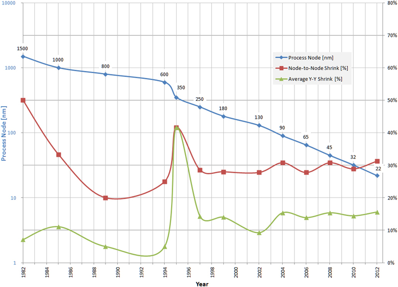
The last decades have witnessed aggressive advances in semiconductor miniaturization. During the 30 years from 1982 to 2012, commercial processes for fabricating CMOS logic shrank from the 1.5 μm node to the 22 nm node (see Figure 1). The resulting increase in functional-density—more than 4,600:1—has altered the course of electronic product design, not just within computational cores or memory subsystems, but throughout the product as well.
Click image to enlarge
Figure 1: In three decades, commercial semiconductor processes for fabricating digital circuits have moved from the 1.5 μm node to the 22 nm node, shown here on a logarithmic scale (left).
At the start of this interval, typical electronic products provided low functional density and presented modest power demands, so power supply designs made use of discrete components and less than optimal cooling methods. Although supply efficiencies were poor by today’s standards, they were sufficient given their products’ low power requirements and large enclosure size.
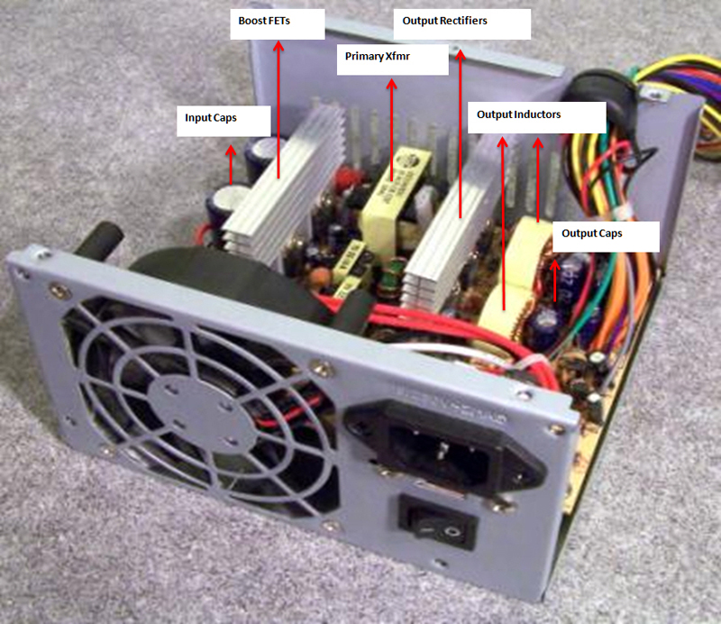
Among the best-known examples of these designs that remain in use today are the silver-box supplies that power desktop computers. For example, a 400 W ATX12V features a largely discrete design (see Figure 2). Individual heatsinks cool power MOSFETs and output rectifiers but the overall thermal design results in large thermal gradients, which are problematic at high ambient temperatures. With a typical efficiency of 80%, the 138 x 86 x 140 mm form factor provides a power density of only 0.24 W/cm3. ATX supplies meeting the 80-plus platinum criteria can almost double that number to 0.42 W/cm3 but are still insufficient in power density and not practical for most central office and data center applications.
Click image to enlarge
Figure 2: Traditional open- and closed-box power subsystems, including the ATX12V silver box power supply shown here, provide low power density and limited scaling potential.
Slick as a Brick
A number of alternative structures arose in attempts to optimize power subsystems for various physical arrangements of loads. For example, high up-time applications, such as communication line cards, replaced large, inefficient, multi-output supplies with distributed power architectures. These designs begin with redundant single-output AC-DC converters to ensure that the reliability of the distributed voltage, typically 48 V, meets the system’s uptime requirements. Line cards usually use on-board brick converters followed by a number of small non-isolated point of load (POL) regulators to power individual resources.
Largely discrete, forced-air-cooled power subsystems present uneven surfaces to the cool-air source resulting in turbulent airflow, which can lead to thermal shadowing and hotspots. Encapsulated brick converters use potting compounds to form essentially isothermal devices. Within the encapsulant, power devices thermally couple to an aluminum baseplate, which provides a single cooling surface. Cooling can proceed by conduction, forced-air convection, or a combination of both.
The baseplate surface provides a large contact area for heat-sink attachment. This thermo-mechanical design allows a 600 W max output power from a 117 x 55.9 x 26 mm package and 12.7 mm heatsink (inclusive) for a power density of 3.5 W/cm3—an order of magnitude improvement over closed-frame silver-box designs.
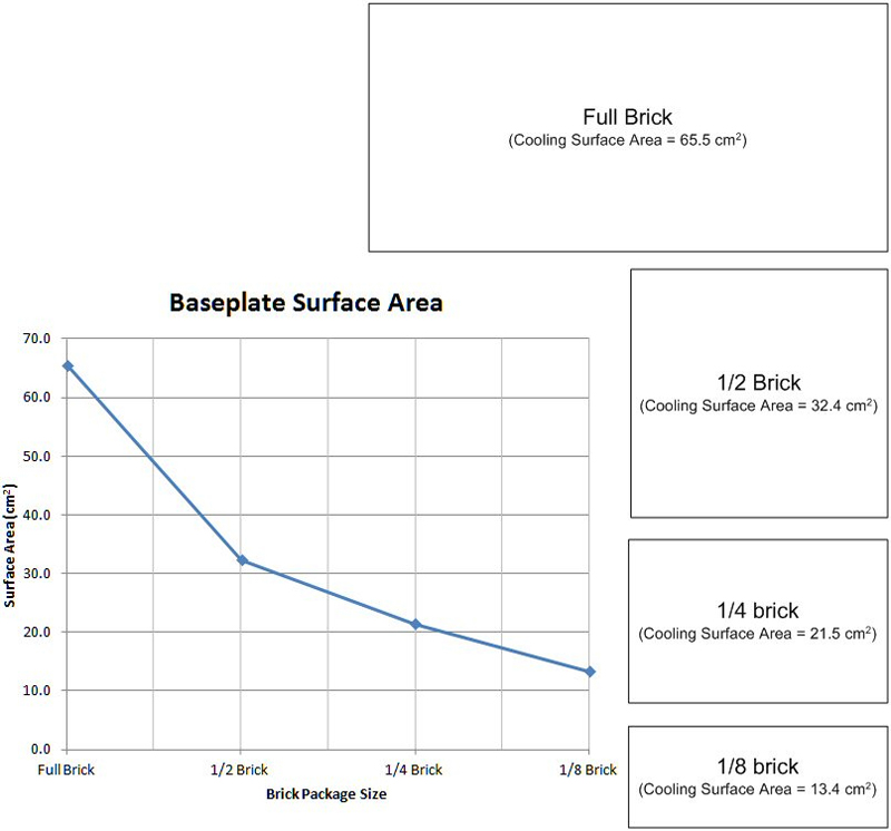
As product functional densities continued to increase, the brick form factor quickly gave rise to fractionally sized versions—half, quarter, and eighth-brick—while successive generations provided increasing power capabilities. The fractional-brick’s shrinking cooling surfaces constituted a thermal challenge for system designs pushing both functional and power densities (see Figure 3). This challenge was exacerbated in applications for which typical ambient temperatures were on the rise as was the case, for example, in server farms and communication hubs.
Click image to enlarge
Figure 3: Fractional brick power management components offer decreasing baseplate surface areas while successive generations increase power density. Thermal challenges result when designs reach practical limitations of single-sided cooling methods.
Most Like it Cool
By now, the functional density of most electronic applications make thermal design an important part of new-product development. The current demands and current dynamics that characterize most products requires embedding the power management subsystem within the functional design—a break from the tradition that held subsystems as freestanding objects.
With electrical loads—heat dissipaters—and power management components (1-η dissipaters) co-locating on system boards, thermal challenges grow with increasing operating temperature: Excess heat reduces the reliability of electronic components. Additionally, designers must derate power components for operation at elevated temperatures so, without effective methods of eliminating heat, power trains become over designed, resulting in larger, heavier, and more expensive systems.
So, as significant an advance as brick packaging technologies were, and while the brick form factors still play a role in terms of simplicity, the industry has grown to need even more dense power management devices beyond what can be accomplished with purely single-sided cooling.
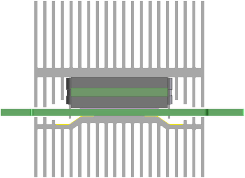
One example of advanced packaging that improves power processing and delivery performance is the Converter housed in Package (ChiP) technology from Vicor. ChiP-based devices exploit symmetrical configurations placing dissipative devices on both sides of a central PCB. A thermally conductive encapsulant transfers heat to both the top and bottom surfaces effectively doubling the cooling surface area relative to the device’s PCB footprint (see Figure 4). With appropriate system PCB design, additional heat can conduct through the electrical contacts as well.
Click image to enlarge
Figure 4: Advanced packaging technologies, such as Vicor’s ChiP, support symmetrical thermal designs exploiting top- and bottom-side cooling.
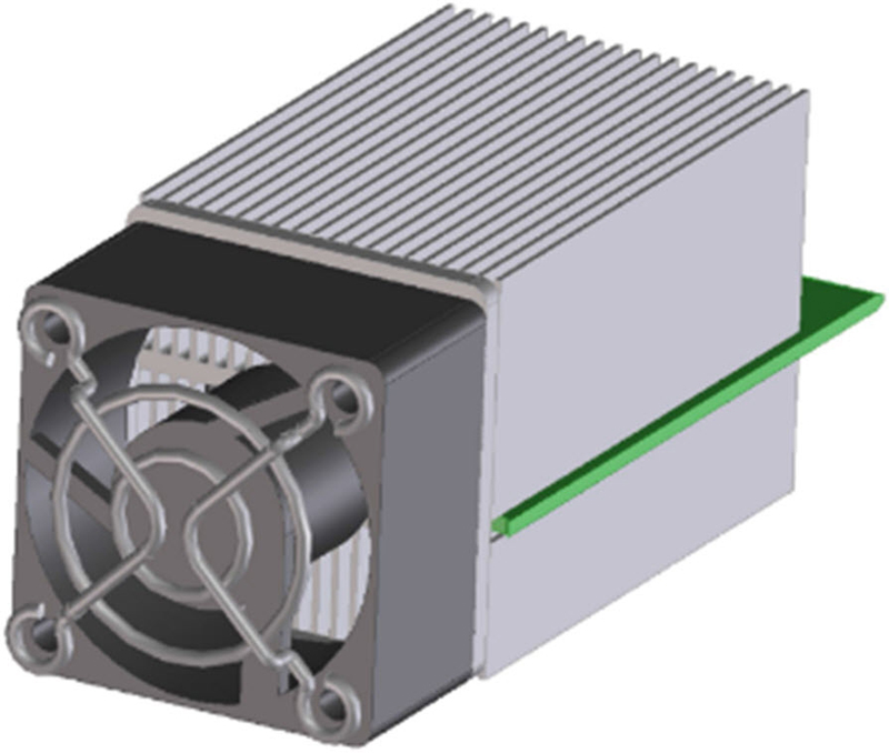
A combination of high efficiency—97.5% peak for 380 to 12 V bus converters—and symmetrical thermal design with advanced materials can provide 1.5 kW. Including heatsinks and a fan assembly, a 40 x 40 x 100 mm assembly offers a power density of 9.4 W/cm3 (see Figure 5).
Click image to enlarge
Figure 5a: Power management devices taking advantage of advanced packaging can deliver as much as 1.5 kW from cells measuring less than 10 in3 including heatsinks and fan.
Click image to enlarge
Figure 5b: Power management devices taking advantage of advanced packaging can deliver as much as 1.5 kW from cells measuring less than 10 in3 including heatsinks and fan.
Advanced packaging technologies such as this provide 3-D thermal management schemes in either surface mount or through-hole mount form factors. Integrated magnetics promote designs requiring few external components, saving design-cycle time, circuit board area, and product assembly costs.
The encapsulant promotes efficient heat transfer while providing a level of safety insulation commensurate with high-voltage power management requirements and international safety standards. This allows the same packaging technology to apply to a wide range of power management functions. These include AC-DC conversion with power-factor correction; isolated bus conversion; DC-DC conversion; buck, boost, and buck-boost regulation; and POL current multiplication. A single packaging technology that is applicable to the full menu of power management tasks from power entry to POL can also simplify system thermo-mechanical design by unifying device profiles and thermal characteristics.
Capabilities and scaling vary among various power component manufacturers, so check your vendors’ offerings carefully. In the case of Vicor’s ChiP-based components, devices can attain thin profiles to 4.7 mm and footprint areas from 6 x 23 mm to 61 x 23 mm, and expanding. Current capabilities extend to 180 A and operating voltages to 430 V, and rising. The company has demonstrated power delivery capabilities in this package technology as great as 1.5 kW, and that number is set to increase as well.
In lower-power applications such as POL converters, small-footprint, low-profile packages provide system designers with additional flexibility to minimize trace lengths from power converter to load. When powering digital resources characterized by high dynamic currents, such as ASICs, processors, or memory subsystems, low loss and low inductance power feeds ensure tight regulation and rapid transient response measured at the load, where it counts.
This type of packaging technology also supports high voltage-ratio converters, which in some applications can allow designers to eliminate an entire conversion stage, reducing system cost, increasing the power-train’s end-to-end operating efficiency, and increasing reliability.