Packaging innovation leads to vastly improved cooling and thermal management
No matter the technical innovation or application, all modern technologies have one thing in common; they rely on a reliable, small and high performance power supply to be able to function and meet their specification. As end products become more complex, the design parameters for the power supply become more challenging, generally requiring more power and more efficiency in an ever smaller space – and with rising energy costs, efficiency is on the agenda of every power supply designer.
Power supply topologies have been developed and improved over many years, and now the focus is turning to the semiconductor devices that are so fundamental to the operation and performance of modern switch-mode power supplies (SMPS). Significant investment has been made to develop devices that switch more efficiently and faster, allowing SMPS design engineers to meet their goals.
However, packaging of switching MOSFETs has continued to lag behind mainstream technologies with many devices remaining through-hole devices (THD), which brings advantages and disadvantages.
In this technical article, Infineon will delve into the topic of semiconductor packaging for SMPS applications and look at how improvements in thermal management and packaging are making a significant contribution to achieving the performance required for modern SMPS.
In order to meet the common goals of modern SMPS designers including fast switching, high efficiency, reduced size and weight and minimized total cost of ownership (TCO), semiconductor materials have been the subject of significant development activity. By driving down on state resistance, improving gate charge and reducing switching losses, the latest superjunction (SJ) MOSFET technologies in combination with the improved CoolSiC™ Schottky diode technologies address these challenges in modern hard- and soft-switching applications.
Despite the advances in semiconductor materials, until relatively recently, the most common packages used for power switching devices were THD types such as TO-220 and TO-247. However, these package types had some significant drawbacks, especially in modern SMPS. The long leads led to parasitic inductance that reduced switching speeds, meaning that associated magnetic components were larger and more expensive. And, with almost all other components on the printed circuit board (PCB) being surface mount devices (SMD), these THD components required a special process step to fit them into the PCB and solder them, increasing production complexity and cost.
Despite all the advantages of currently available SMD devices, such as shorter leads and easier handling in production, they still have some drawbacks with respect to cooling. Currently, SMD devices are generally cooled by contact with the PCB, either through their body or the component leads. This remains one of the major challenges for applications such as power factor correction (PFC) circuits, and is the main reason that TO-220 and TO-247 remain the most common package types used for high power SMPS applications.
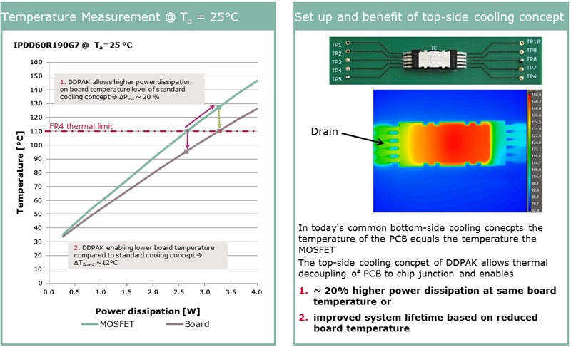
Top-side cooling of SMD
Heat rises and, while conventional SMD packages that disperse heat down into the PCB have some merit, definitely a package that can disperse heat towards its top surface will have better performance as it is working with physics and not against them.
The new Double DPAK (DDPAK) package from Infineon Technologies is a recent example of a surface mountable package for power devices that delivers top-side cooling. The packaging concept is optimized for high power, high voltage and high reliability applications and is suitable for both MOSFETs and SiC diodes, bringing a new direction in terms of power system integration.
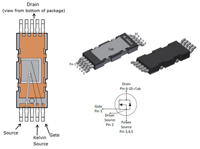
Click image to enlarge
Figure 1: DDPAK technology incorporates top-side cooling in an SMD package
Most commonly, the DDPAK offers five connections for the drain current, three source connections and one source sense connection for the gate reference potential, as well as a single connection for the standard gate drive. Although this 4-pin approach is possible with conventional THD packages and would allow for electrically cleaner driving signals that reduce switching losses in the application, THD device space constraints still remain an issue.
This is further improved by the lead inductance being reduced by 50% of the SMD package size.
The DDPAK is smaller than the TO-220 package, thereby saving space and allowing greater power densities to be achieved. This is further helped by the 18% improvement in thermal coupling between the semiconductor junction and the case.

Click image to enlarge
Figure 2: DDPAK offers significant size and performance improvements over TO-220
The thinner form factor is also highly compatible with modern product designs, allowing for thinner end products to be designed.
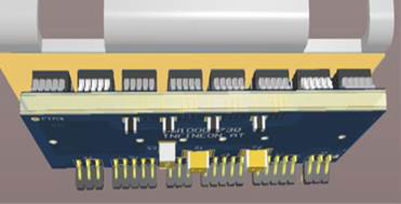
As the body of the DDPAK is not in direct contact with the surface of the PCB (with approximately 150 µm between the two) further benefits and flexibilities are delivered to the designer.
Click image to enlarge
Figure 3: Separating the DDPAK from the PCB offers advantages and flexibility for designers
Many product safety standards, especially those for power supplies, such as standards from Underwriters Laboratories (UL) stipulate the maximum temperature that a FR4-based PCB can reach during operation. When the semiconductor device (e.g. MOSFET, SiC Diode) is in direct contact with the PCB this rule limits the temperature of the semiconductor, thereby constraining the performance of the SMPS.
One challenge with conventional SMD packages that are mounted on PCBs is the different rate of thermal expansion of the device / package and the PCB itself, due to the different Coefficients of Thermal Expansion (CTE) of the two materials. A specific test (known as Temperature Cycling On Board (TCOB)) is defined by IPC9701 to address this issue.
As the leads on a DDPAK are compliant, they have a certain spring-like quality and act as a buffer between the body of the DDPAK and the PCB. This innovation completely eliminates CTE-related failure modes including solder joint fatigue and internal package defects due to the stress. In fact, when a TCOB test with over 2000 cycles was performed on a DDPAK there were no failures – indicating a quality level that will meet automotive standards even though it is an industrial product.
Heatsinking the DDPAK
While the DDPAK is thermally very efficient, for almost all practical applications some form of heatsinking is required to be attached to the top-side to assist the movement of thermal energy away from the semiconductor junction and into the ambient surroundings.
Click image to enlarge
Figure 4: Several options exist for attaching heatsinks to DDPAK devices
Selection of the actual heatsink to be used will depend on several factors, although the thermal energy to be dissipated and the available space within the design are generally two of the most important. The design of the DDPAK gives several options for affixing the heatsink to the package including the use of clips, push pins, adhesives or even direct soldering. The final choice will be made depending upon the needs of the design and what suits the production process. As no heatsink face or package surfacecan ever be 100% flat, it is good practice to include some form of thermal pad or thermal paste to ensure a good thermal contact between the DDPAK and the heatsink.
A real world example: 1600 W Titanium server power supply
To illustrate the performance of DDPAK devices we shall consider a 1600 W Titanium server power supply which is a demanding real world application.

Click image to enlarge
Figure 5: The challenging Titanium server power supply specification
The basic hardware construction consists of an input filter, AC/DC conversion stage, control / bias board and DC/DC stage. As is typical for server power supplies, forced air cooling is provided via an inbuilt fan. This directs airflow over the power board that contains the DDPAK devices.

Click image to enlarge
Figure 6: Basic layout of the 1600 W server power supply demo setup
The daughter card contains a full PFC and a half-bridge LLC stage that delivers up to 1600 W of power with an input of 230 VAC. Figure 6 shows the overall design that meets the efficiency 80 PLUS® Titanium standard requirements at 50% load and exceeds them at the other critical load points of 10%, 20% and 100%.
Summary
Designing SMPS is a challenging business and the requirements continue to get tougher as applications demand ever-higher levels of power density and efficiency with each iteration. While the semiconductor materials have advanced dramatically, the package has not kept pace with THD packages remaining the most common in power-related applications.
However, the advent of the DDPAK from Infineon Technologies brings a new packaging concept to the market that meets the needs of even the most demanding applications. Thermal performance is improved due to top-side cooling and switching speed is increased due to a 50% reduction in parasitic inductance.
Furthermore, the innovative mechanical design not only separates the module from the PCB, it also includes compliant legs that remove any of the potential failures associated with CTE.
When combined with the latest silicon technologies, such as CoolMOS™ G7 and CoolSiC™ G6, DDPAK delivers a significant step forward in switching devices for market-leading SMPS.
More detailed technical data on the DDPAK top-side cooled package, along with a dedicated application note, will be available on the Infineon website.