Advanced T-type NPC- 3 level modules: A novel possibility with RB-IGBT’s
A new device structure targets design engineers and program managers looking for the next big game changer
A novel IGBT structure was developed with reverse-blocking capabilities comparable to the forward voltage rating of the IGBT. This new device, known as the RB-IGBT, was used to create a 3 level advanced neutral point clamping power converter that shows better loss characteristics than standard 3 level converters.
The results of loss comparisons performed have been presented along with an application where this new structure has helped improve performance. The presentation is targeted at design engineers and program managers looking for the next big game changer.
Energy is an issue that affects every person on the planet. With the advancement of the Human Race, Energy Dependence has increased and this has strained the Earth’s natural resources. To make better use of the available resources, numerous efforts have been made to improve existing technology and change the way new products and made and used.
Fuji Electric has always been on the forefront of Energy innovation. Our operating philosophy is creation of responsible and sustainable societies through innovation in Energy Technology. In keeping with our long-standing history, innovating and bring to the world advanced solutions which serve the global effort toward a brighter and healthier tomorrow.
RB-IGBTs
Fuji Electric has pioneered this change in the field of Power Electronics, most recently with the introduction of RB-IGBT’s (Reverse Blocking Insulated Gate Bipolar Transistor). The RB-IGBT was developed for use in Matrix Converters, but we have been expanding its target application areas, which now include Current Source Inverter for Motor Drives (EV/ HEV) and 3 level inverters for PV, Wind and UPS.
RB-IGBT’s use in the Advanced T-type NPC (Neutral Point Clamping) 3 level modules give energy efficiency a whole new meaning. The intention of this article is to shed light onto this innovation and expand its use in the market.
Device Structure
A conventional IGBT has forward and reverse blocking capability. So theoretically, we can use the IGBT to block reverse voltages equivalent to the IGBT forward voltage rating. However, practically, this is not true. Under reverse bias, there is a leakage current, the dependence of this current on reverse voltage is exponential.
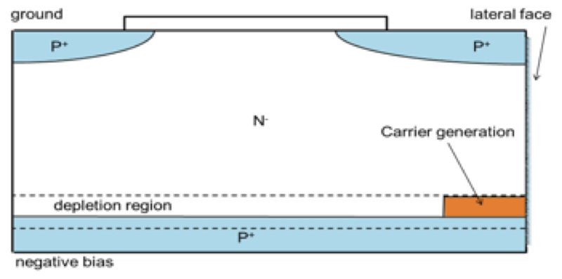
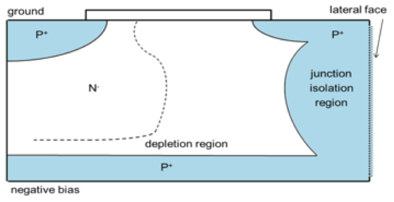
The primary difference in structure between the Fuji RB-IGBT & a conventional IGBT is that the former has deep junction isolation structure that limits carrier generation thereby providing the needed (higher) reverse blocking capability. Figure 1 below shows the cross section of the conventional IGBT and Figure 2 that of the Fuji RB-IGBT.
Click image to enlarge
Figure 1: Cross section – Conventional IGBT
Click image to enlarge
Figure 2: Cross Section – RB – IGBT
There are other ways to achieve reverse blocking – Halo Implants (Selective implantation), passivized sidewall, post treatment of diced IGBT dies to heal the crystal lattice, etc. All the mentioned methods however are not commercially viable and Fuji research found the implanted junction isolation region to be the technology of choice.
The first question to be answered is why there is carrier generation at the lateral face junction and how the junction isolation helps. At the Collector-Drift PN junction, the collector region is more heavily doped, so under reverse bias, the depletion region extends further into the drift region that the collector region.
In a conventional IGBT, this extension extends only part way into the drift region. This combined with the fact that mechanical dicing of the IGBT die damages the crystal lattice, creating carrier generation hot spots. The generated carriers with enough energy enter the drift region and contribute to the leakage current. As the reverse bias increases, the carrier energy increases thereby increasing leakage current.
In the Fuji RB-IGBT, the introduction of the junction isolation region, isolates the crystal lattice defects from the drift region. The E-field also changes significantly and the concave curvature of the junction isolation region helps achieve the required Reverse breakdown voltage.
Performance
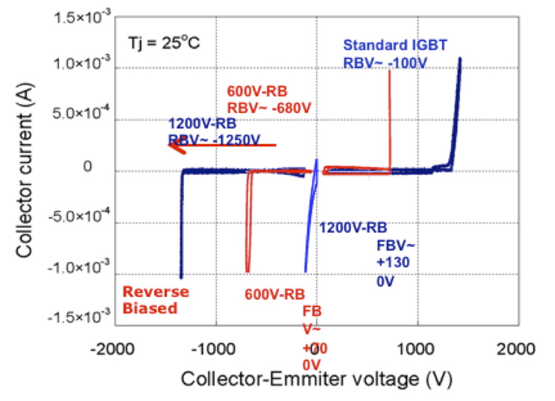
The forward characteristics of the RB-IGBT are very similar to that of a standard IGBT. Therefore switching speed and trade-off curve of Von are similar. Figure 3 shows the reverse characteristics of a conventional IGBT as compared to a RB-IGBT.
Click image to enlarge
Figure 3: The advantage of using RB-IGBT’s – The reverse blocking capability.
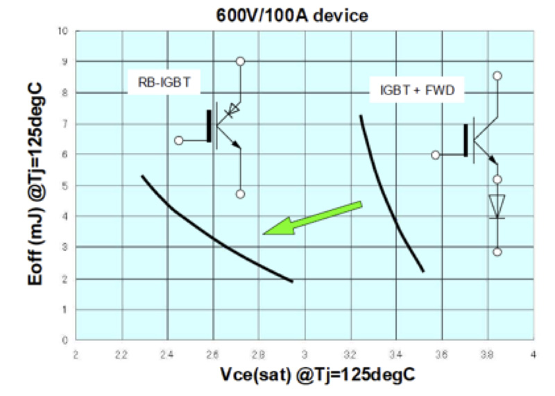
Figure 4 shows the Vce(sat) v/s Eoff tradeoff relationship for the IGBT+FWD & RB-IGBT. There is a significant improvement in Vce(sat) at the same Eoff levels.
Click image to enlarge
Figure 4: Trade-off relationship of RB-IGBT and IGBT + diode.
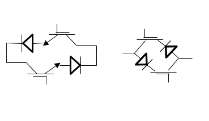
Figure 5 above shows the implementation of an AC-Switch. 5(a) is the AC switch implementation using a conventional IGBT, this requires 4 dies ( 2 IGBT + 2 FWD). 5(b) is the RB-IGBT implementation, which requires only 2 dies (2 RB-IGBT’s).
Click image to enlarge
Figure 5: (a) Conventional AC-switch (b) AC-switch with RB-IGBT
Multilevel inverters
Multilevel Inverters have been in discussion from the early 1980’s. Their end goal is to reduce inverter harmonics and thereby reduce use of magnetic components. An added advantage is reduced losses, with the introduction of NPC, TNPC & ATNPC (Advanced T-type Neutral Point Clamp) topologies.
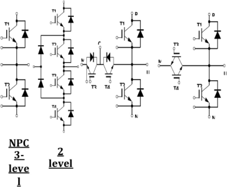
A direct application of the Fuji RB-IGBT is the Advanced T-type Neutral Point Clamped module. The T-type modules in existence/ those offered by our competitors use the conventional AC-Switch shown in 5(a). More components means more losses and more chances of failure. A loss comparison is presented in the next section that details the performance of the 2-level inverter, 3 level NPC inverter, Advanced NPC 3 level inverter and the Advanced T-type 3 level inverter. Figure 6 shows the different inverter topology phase legs that are used for comparison.
Click image to enlarge
Figure 6: Inverter Topologies
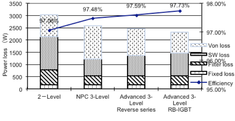
The loss comparison (see Figure 7) is made at the following conditions: Fsw = 10 kHz; Vout = 400 VAC; Iout = 145 A; PF = 1; DC Link Voltage = 660V.The 2-level inverter has the highest loss among the 4 topologies, thereby having the lowest efficiency. The AT-NPC on the other hand has the least loss and therefore the highest efficiency. With the NPC 3-level and ANPC 3-level modules, there is a higher Von loss compared to the 2-level inverters due to the increased number of IGBT’s. With the AT-NPC, there is a trade-off between switching loss and Von loss.
Click image to enlarge
Figure 7: Loss comparison of different inverter topologies
Applications
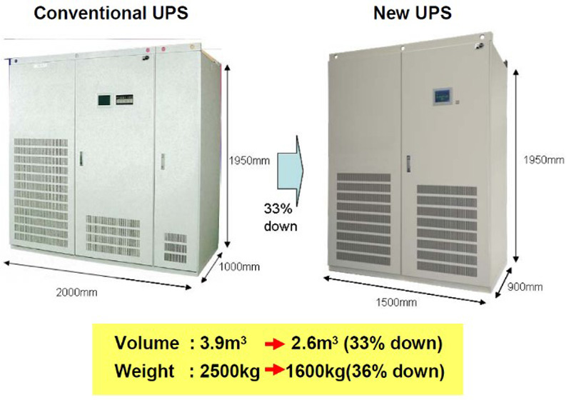
Figure 8 shows the implementation of a conventional IGBT in a classic 2 level configuration in a 500 kVA UPS v/s the application of RB-IGBT in the Advanced T-type configuration for the same application. There is a significant performance improvement with an efficiency increase of 2% from 95.1% to 97.1%. There is also an added benefit of a 33% volume reduction, weight reduction of 36%, due to the reduction in filter components & magnetics. Target application areas include matrix converters, current source inverters for motor drives (EV&HEV), and level Inverters for PV, Wind and UPS.
Click image to enlarge
Figure 8: Before and after