Advancing flexible encapsulation tech empowers flexible electronics
In 2020 flexible barrier manufacturing for flexible electronic devices such as displays will be a market worth more than US$184 million, according to IDTechEx Research. That equates to 3.8 million square meters of flexible barrier films for electronics.
Although multilayer approaches – usually organic and inorganic layers – have been the most popular solution for flexible encapsulation so far, there is significant development work with solutions based on single layer approaches such as flexible glass or atomic layer deposition (ALD) which could, in later years, capture part of the market. The table below, compiled by IDTechEx analysts shows some of the characteristics of flexible glass and ALD films as developers are looking to bring them to market.
Flexible glass: current status, outlook and challenges
Flexible glass is a significant technical achievement yet IDTechEx Research believes that it will not be the solution of choice for encapsulation of flexible electronics in the short to medium term, for multiple reasons.
In spite of the marketing spin given by the manufacturers, glass is inherently a fragile material and requires specialized handling and processing. While plastic materials can also be damaged, there is an important difference between the two: damage of barriers on plastic can lead to the failure of a specific part, however, shattering of glass, even if protective sheets are used, leads to particle contamination on the defect line able to affect multiple parts.
Inherent fragility of flexible glass makes sheet edges critical. All suppliers propose protective tabs to reduce the problem. However, any other particle on the processing equipment could also become a focal point of stress and lead to shattering of the glass sheet or web.
A strong point of traditional glass encapsulation (especially for top emission devices) has been its ability to form truly hermetic packaging by using glass frit and laser sealing. This advantage may not be transferable to flexible glass where glass-to-glass sealing may be very problematic and difficult because points of stress and relative twisting of the two sheets must be avoided in the laser firing of the frit. It may be that flexible glass has to be used in combination with adhesives (and desiccants).
Flexibility is another issue. Although glass is very flexible if flexed along a well-defined axis, it can be poor at tolerating any stress out of axis, so much so that twisting the sheet may lead to fracture. This is true with or without protective film applied to the glass. Extreme flexibility (r< 2-3 mm) may also be a problem. Data that has been shown would put the flexibility limit around r= 2.5 cm. Consequently, flexible glass as an encapsulant superstrate or substrate may be good for conformal applications, but for truly flexible applications there seem to be several challenges to be overcome.
Flexible glass makers are also waiting for equipment providers to make appropriate equipment to handle the flexible glass in manufacturing, another bottle neck.
Future opportunities for flexible glass
The thermal stability of flexible glass makes it the best choice as substrate for back-planes of high-resolution high-end large displays. Glass enables improved resolution and good registration between layers during processing compared to plastic substrates like PET, PEN, and PI. However, IDTechEx analysts and other affiliate experts have only seen results with metal oxide backplanes only so far (Tprocess < 350 C), none with LTPS backplanes (Tprocess < 450 C). If processability up to 450C is indeed possible, flexible glass would be a very good choice as a substrate for flexible AMOLED TV. Those devices are bottom emission (BE) AMOLED, normally have a metal foil as back encapsulant, a higher cost tolerance. Regarding R2R processing of flexible glass, it has demonstrated possible. Manufacturing by R2R will require specialized tools not differently than fabrication of barrier in R2R.
The multi-layer approach if correctly implemented on dedicated tools may have the potential to be low cost but an open question remains as to how low the defect density of barrier on foil can be. Consequently, it is an open question what the maximum size of displays that can be encapsulated with compatible yield can be. As it transpires from the discussion above, plastic engineered superstrate (=encapsulant foil) may be better for smaller devices (wearable, phone, tablets), while flexible glass may be better for TVs and in general larger displays.
Additionally, the smoothness of plastic films, even with smoothing layers, is not as good as glass (0.2 nm). This may be a problem for organic TFT backplanes. Finally optical transmission below 400nm require glass as substrate since PET and PEN have a cut off around 400 nm (PEN). IDTechEx does not see this as a critical limitation for general display applications (it may be for OPV).
Atomic layer deposition (ALD) present and future outlook/market share
ALD is another flexible encapsulation technology receiving a lot of attention with several players currently developing solutions based on it. It seems like it is not a short-term solution, if it will ever be one as a stand-alone layer but ALD may be a solution in a multi-layer stack in combination with a sputtered or PECVD layer if it would be possible to find a good cost structure. Regarding the intrinsic properties of the material, ALD film deposited at low temperature (T<80 C) have a superior quality when tested at room temperature. A single ALD layer less-than 50 nm thick can perform better than thicker layers deposited by sputtering or PECVD.
However, the inherent stability of the films at higher temperature/humidity (e.g. 85C/85%RH) is a problem. If PE-CVD is used, ALD film stability improves, as well as for mixed oxides, but it is still an issue. A second problem comes with particles and substrates non-uniformity. Any defect may lead at an initial non-uniform nucleation that propagates into the growing film. Furthermore, loose particles on substrates may be partially covered, but because of the extreme thinness, the thin film does not have the mechanical strength to keep them in place under mechanical stress. Any mechanical stress leads to film fracture with consequent creation of an ingress path for moisture. That is why multilayer structures are necessary.
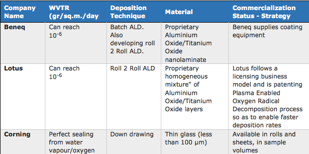
Deposition tools are in development from Lotus, Beneq, Encapsulix and others. Exploration at Samsung SDC with ALD films for TFE was very much advertised by Synos, but resulted in failure and any further evaluation was halted. ALD for barrier on foil has better results although there are doubts and hurdles in scaling up and reaching the deposition speed required for a cost effective process.
For more read the full analysis of the topic including ten year forecasts by each application type and profiles of the key suppliers in the report “Barrier Layers for Flexible Electronics 2015-2025”.
Printed Electronics USA (November 18-19 at Santa Clara, CA)