Advancing Power Density for Hi-Rel Applications

To optimize a system, you must first understand it. Only then can you apply the required remedies to address the challenges presented.
Designing power systems is never easy. With today’s pressures on power density and efficiency - especially in battery-driven devices - even designing a power supply for general applications takes a lot of effort. High-reliability, military and aerospace applications, add extra demands such as the need for extreme environment survival, electronic noise and leakage, and other mission-oriented demands.
Another key consideration for mil/aero systems is that power systems must be as light as possible, resulting in an often-conflicting set of parameters to be met. Increases in power density often create thermal management issues, for example. In order to increase efficiency, power density, and environmental ruggedness it is important to use the best materials, technologies, and topologies available.
Looking for the losses
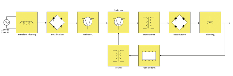
In electronic systems, we need to identify where losses occur in order to determine what needs to be done to reduce them. Finding the issues in a circuit lets you focus on the major contributors to inefficiency, and eliminate or minimize them. Most legacy power supplies have seven major areas of interest, or blocks, each with their own associated losses (Figure 1).
Click image to enlarge
Figure 1: Most legacy power supplies have seven major areas
One issue to be faced when designing a power supply is that you can’t create the source that it runs from. Most of the losses in the first block (transient filtering) in Figure 1 are principally I2R losses; not much can be done here except to increase the cross-sectional area of the conductors to reduce resistive losses. Halving voltages at this stage will inherently have a squared increase in the losses induced, so the supply voltage should be as high as possible.
The diodes in the traditional rectifier bridge in block two each have a voltage drop across them. A full wave rectifier has the added disadvantage of needing two diodes in series to achieve full wave rectification. These losses can be mitigated by using high-performance components like wide-bandgap diodes made from Silicon Carbide (SiC).
Block three in this circuit is where the input voltage is boosted to a higher voltage, normally in the range from 360Vdc to 400Vdc. There are several areas of loss within a PFC circuit: resistive losses within the inductor; switching and resistive losses due to RDS(on) in the Q FET switch; and switching and forward voltage drop losses in the rectification diode. The higher the working voltage of the circuit, the more you can reduce losses, because the current is the major contributor to loss in the circuit.
The fourth section is the drive circuit for the main isolation transformer. The losses that can be found here are switching losses in the FETs and resistive and switching losses in the FETs due to RDS(on); in block five, we see resistive losses in the transformer’s primary and secondary coils. In block six, rectification, there are two types of switching losses, the forward voltage drop and switching losses of the diodes. Smoothing and Filtering is in block seven, and if the power supply is designed well, the losses here should be minimal.
It’s the switching
In most basic converter topologies, semiconductor losses tend to cause the largest degradation of efficiency. The MOSFETs and diodes in both are victims of two varieties of power loss: conduction and switching. Scotty from Star Trek often said you can’t change the laws of physics, and the same is true in this case. Where there is current flowing, there will naturally be a resistance, with energy wasted (losses) as a result. In switching, both the MOSFET and the diode route current through the circuit when either device is on, with losses generated due to the on-resistance of the MOSFET and the forward voltage of the diode.
Since MOSFET current flows only while it is on, MOSFET conduction loss is approximated by the product of RDSon, duty cycle, and the square of on-state current:
PCONDmosfet = IMOSFETon(avg)2 x RDSon x D
where IMOSFETon(avg) is the average MOSFET current over the on-interval. PCONDmosfet = IOUT2 x RDSon x (tOFF / tON)
While MOSFET conduction loss is proportional to the dissipation across its low RDSon, diode conduction loss is dependent on a comparatively-larger forward voltage (VF). Thus, diodes usually have a larger conduction loss than MOSFETs. Diode conduction loss is proportional to forward current, VF and conduction time. Since the diode will conduct when the MOSFET is off, diode conduction loss (PCONDdiode) is approximated as:
PCONDdiode = IDIODEon(avg) x VF x (1-D)
where IDIODEon(avg) is the average diode current over the on-interval. PCONDdiode for a stepdown converter is estimated as:
PCONDdiode = IOUT x VF x (1 - tOFF / tON)
By observing these equations, it is evident that the longer either device is on during each switching interval, the larger that device’s relative conduction loss. For a step-down converter, the lower the output voltage is set (for a constant input voltage), the more the diode contributes to power loss, since it conducts for more of the switching interval.
MOSFET and diode losses are mostly due to their switching characteristics. Energy ramp-up over time is needed for the devices to transition from fully Off to fully On, which translates into power consumption as the devices change state.
A simplified plot of drain-to-source voltage (VDS) and drain-to-source current (IDS) is usually given to explain the switching loss encountered in MOSFETs. The upper plot in Figure 2 depicts such waveforms, where non-instantaneous voltage and current transitions occur during tSWon and tSWoff due to the charging and discharging of capacitances found in the MOSFET.
As shown in Figure 2, the full-load current (ID) must be transferred to the MOSFET before its VDS decreases to its final on-state value (= ID x RDSon). Conversely, the turn-Off transition demands that VDS increases to its final Off-state value before current is transferred from the MOSFET. These transitions result in overlap of the voltage and current waveforms and lead to the power dissipation seen in the lower plot in Figure 2.
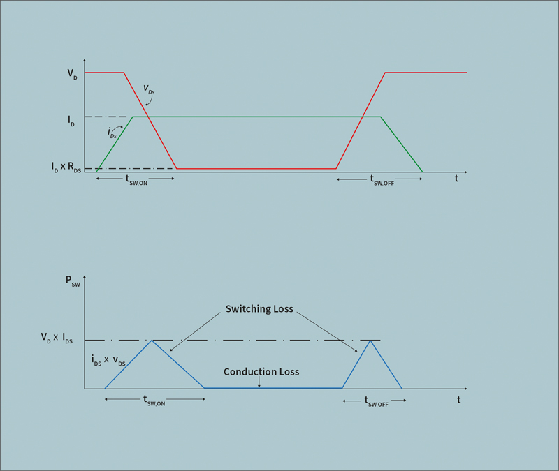
Click image to enlarge
Figure 2: A simplified plot of drain-to-source voltage and drain-to-source current
Switching transition times are more or less constant over frequency, causing switching loss to increase as the frequency of the SMPS is raised. This can be understood by noting that the constant-transition periods consume a greater proportion of the available switching period as that switching period shrinks. A switching transition that requires only one-twentieth of the duty cycle will have much less of an effect on efficiency than one that consumes one-tenth of the duty cycle.
Due to its frequency dependence, switching losses dominate conduction losses at high frequencies. MOSFET switching losses (PSWmosfet) are estimated by applying triangular geometry to the figure above to achieve following equation:
PSWmosfet
0.5 x VD x ID x (tSWon + tSWoff) x fs
where VD is the drain-source voltage of the MOSFET during Off-time, ID is the channel current during on-time, and tSWon and tSWoff are the turn-On and turn-Off transition times, respectively. For the step-down converter, VIN is applied across the MOSFET during the Off-state, and it carries IOUT while it is On.
Addressing the issues
When it comes to the rectification in a circuit, active switching elements can be used instead of diodes, as they have no forward voltage drop - there is, however, an RDSon to consider. Here again, switching (no pun intended) to a wide-bandgap solution for the switches can also benefit. In the area of Active Power Factor Correction, the major energy thief is the diode’s high switching losses. The easiest solution here is also to migrate these devices to wide-bandgap alternatives, as they inherently have lower switching losses.
Additional solutions
A good option to address system efficiency is to use a combined solution of rectification and Power Factor Correction with a bridgeless PFC in single-phase systems. In the area of power magnetics, using a resonant topology and planar transformer technologies can provide significant improvements.
This brings us to the issue of operating frequency. Although we stated that an increase in frequency also increases switching losses, migrating to wide-bandgap devices enable higher frequencies to be used without significant penalty. Since gallium nitride (GaN) devices have very minimal switching losses compared to silicon FETs, they also enable an increase in switching frequency, allowing a reduction in the physical size of the magnetics. Reducing the volume of the inductors and transformers in a circuit not only increases power density, it also reduces the resistive losses as there is less resistance in a lower-inductance coil.
A single-stage solution
Changing the topology from multi-stage to single-stage removes blocks four and five from Figure 1, and all the associated losses. Such a topology has a PFC with a transformer in place of the inductor to create an isolated secondary circuit. One development process could be to consider a PFC that is capable of modification to a single-stage topology, then start with a silicon solution at normal operating frequencies, then migrate to a higher operating frequency based on a wide-bandgap device.
Recently, On-Systems has introduced a new PSU platform, combining a new topology, custom-designed FET drivers, and a fast switching speed to deliver industry-challenging benefits. Incorporating the latest in materials and technologies, the rugged, EMI-silent PSUs provide the same or better performance of a legacy supply in less than a quarter of the space, a third of the weight, and less than a half the cost. The first product is called Pebble, a laptop PSU that measures just 115 x 52 x 36mm, weighs only 180g, and meets all applicable MIL-STD and DEF-STD regulations at 20% the cost of existing solutions (Figure 3). By comparison, legacy electrically-‘silent’ supplies for use in secure, harsh environments are about the same size as the laptop that they power and weigh from two to three kilos.

Click image to enlarge
Figure 3: The Pebble laptop PSU measures 115 x 52 x 36mm and weighs only 180g
The rugged, EMI-silent COTS Pebble laptop power supply is the first in a series of harsh-environment PSUs from the company which use a new topology, custom-designed FET drivers, and a fast switching speed to deliver significant benefits. Combining three stages into one, the design not only reduces I²R losses while increasing efficiency, it also uses advanced fast FET drivers to operate at up to 40x typical switching frequencies, reducing the size of EMC filtering components required.
The laptop PSU meets all defence EMC performance standards, including MIL-STD 1275A-E, MIL-STD 704A-F, DEF-STAN 59-411 and MIL-STD 461 E-F EMC. The 96% efficient Pebble accepts universal AC and wide DC input, with features like short circuit, overload, and overvoltage protection.
Looking forward
With the advancement in core technologies and materials, there are a growing number of new and novel techniques in power conversion that can now be brought to bear to address the issues of power density, efficiency, and performance in a mil/aero environment. The latest wide-bandgap devices and the topologies they enable bring the promise of higher operating efficiencies, better efficiency, and improved performance.
On-Systems
www.on-systems.co.uk