Affordable RMS Power Meter, Operating from 100 MHz to 40 GHz
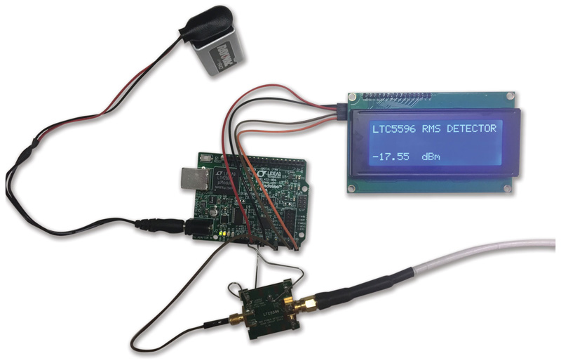
Figure 1. A complete broadband RF power meter
RMS-responding RF power meters are widely used in test and measurement applications to precisely and accurately measure the RF power of signals with varying crest factors. These expensive connectorized devices offer a high level of precision, while relying on extensive characterization and calibration, but this precision comes at a cost in size and expense. For far lower cost and much smaller size, the LTC5596, a 100MHz to 40GHz rms responding integrated circuit with 35dB or more detection range, can be used to build a handheld broadband power meter, or even in-circuit, embedded power meters.
The LTC5596’s well-controlled linear-in-dB transfer function and excellent flatness vs. frequency allows for easy calibration—as basic as a single midfrequency two-point calibration, resulting in ±1 dB of measurement accuracy across a frequency range from 150MHz to 30GHz. The LTC5596 low power consumption (only 100 mW) and its integrated nature make possible in-circuit and handheld power monitoring solutions.
The simplicity of a complete solution is illustrated by the battery-powered example of Figure 1, where a broadband RF power meter can be built using the available LTC5596 demonstration circuit (DC2158A), an I2C LCD display, and the DC2026C Linduino board running a short firmware program (see Appendix).
Click image to enlarge
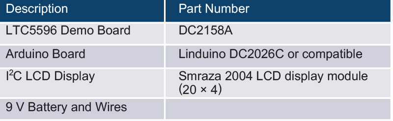
Table 1. Bill of Materials
Circuit Assembly
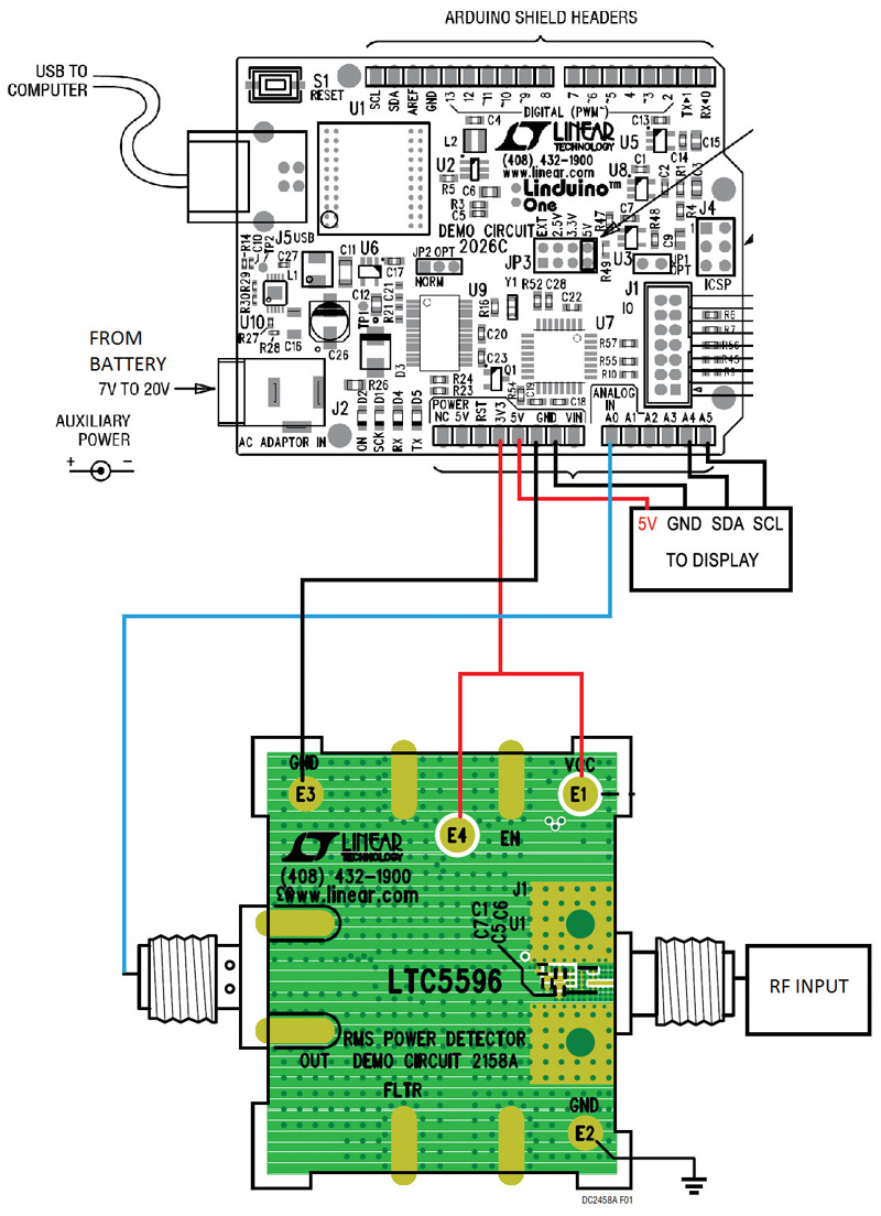
Figure2 shows the assembly scheme. The Linduino board has multiple ADC inputs in the analog IN bank — A0 is used here to sample the output of the LTC5596 detector. The display features an I2C interface, which simplifies connections to the Linduino board. The complete circuit is powered through the Linduino board’s auxiliary portion, including the LTC5596 board and connector.
Click image to enlarge
Figure 2. Connection diagram
Firmware
All of the required firmware runs on the Linduino board. The main function of the firmware is to convert the measured analog input (volts) to RF power (dBm) and display it on the LCD display. To do that, a two-point calibration is recommended to find the slope and intercept point of the LTC5596’s linear transfer function — VOUT vs. RF power in the linear form:
where x is input power in dBm, y is the LTC5596’s output voltage (VOUT) that is directly proportional to the ADC code, m is the slope, and b is the x-intercept (VOUT reaches 0). The firmware calculates x based on the measured y, with the values of b and m coming from calibration (explained below). Averaging multiple readings can help minimize the effects of noise.
The Linduino’s onboard ADC has 10 bits of resolution, corresponding to an LSB size of about 4.9 mV. The typical slope of the LTC5596 is 28.5 mV/dB, resulting in a measurement resolution of approximately 0.2 dB. The Appendix shows sample firmware code that is used for 5.8 GHz to display the input power in dBm.
Calibration
Although the LTC5596 features a linear-in-dB transfer function. Part-to-part variations result in a range of transfer function slopes and axis intercept points. Since the transfer function is linear, calibration is simple, requiring only two-point calibration (or more, if desired) to assure accuracy.
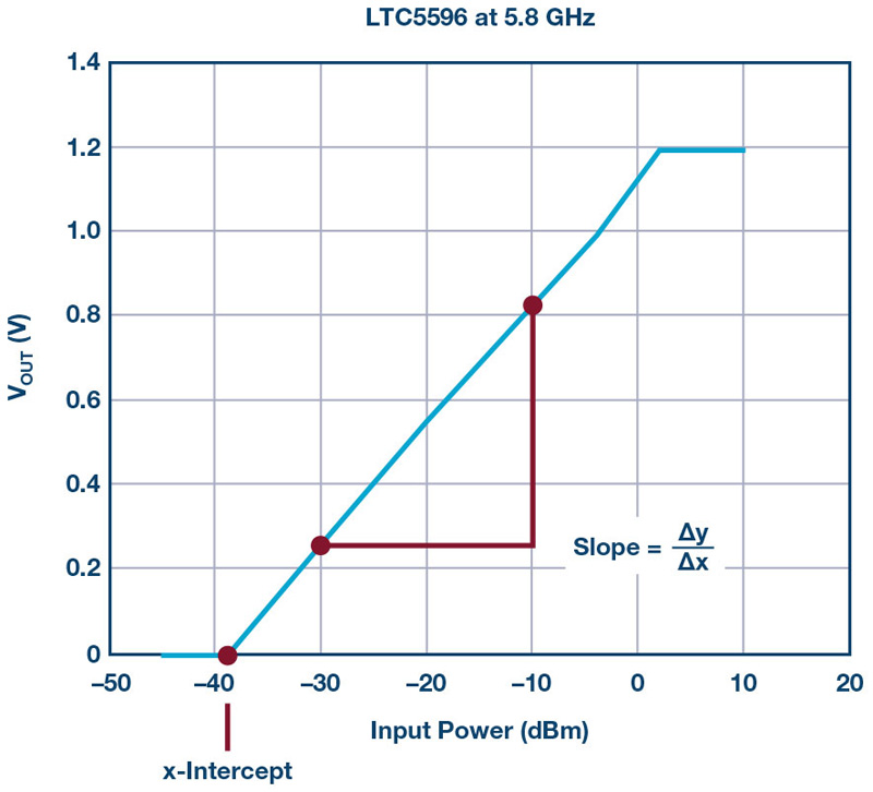
Figure 3 shows two-point calibration of a typical transfer curve taken from LTC5596 at 5.8 GHz. The two points are used to derive the slope and x-intercept.
Click image to enlarge
Figure 3. LTC5596 VOUT vs. input power. The two calibration points should be chosen to represent the operating range of the application
In this example,
These slope and intercept values are used in the code that’s shown in the Appendix.
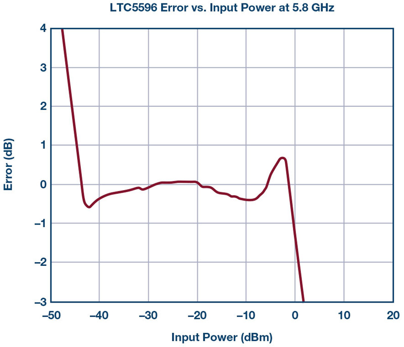
Linearity Error
In the data sheet, the log intercept is the x-intercept point on the plot. Linearity error is the difference between the ideal straight line and the actual measured power by the detector. The useful detection range is typically where the linearity error is less than 1 dB. Hence, error can be calculated using the x-intercept point and the slope shown in Figure 4, which shows the linearity error of a typical device a system can achieve with two-point calibration.

Click image to enlarge
Figure 4. LTC5596 error vs. input power after calibration. The linear dynamic range can be seen as approximately –40 dBm to +3 dBm.
Conclusion
The LTC5596 brings small size, unprecedented simplicity, and lowpower requirements to accurate RF power metering in the 100 MHz to 40 GHz range. It makes possible complete solutions that are small, efficient, and accurate enough to satisfy the requirements of a portable handheld RF power meter, or even act as in-circuit, embedded RF power meters. Firmware overhead is minimal because of the well-behaved and broadband transfer function of the LTC5596, which is linear-in-dB. Two-point calibration can be performed at a single mid-band frequency with good accuracy, or at more frequencies for improved accuracy. More importantly, the LTC5596 rms detector is capable of accurately measuring the power regardless of the type of modulation. Even with simple two-point calibration, the results are accurate—less than 0.3 dB of error independent of the modulation waveform. In contrast, other expensive commercial units require extensive calibration and characterization.