Author:
Hubert Baierl, Marketing Director, Infineon Technologies
Date
10/20/2025
 PDF
PDF
Click image to enlarge
Figure 1: EOS worst case – high-side gate drain short whilst the low-side is on
Achieving a 100 W/inch3 power density in an 8 kW SMPS, with a 97.5% peak efficiency and a compact 1U form factor can be quite the design challenge. But it is now within reach thanks to a smart combination of switching devices:
· PFC stage: 650 V silicon carbide (SiC) MOSFETs (Infineon’s CoolSiC™)
· LLC stage: 650 V gallium nitride (GaN) power switches (Infineon’s CoolGaN™)
· Synchronous rectification and ORing stages: 80 V MOSFETs (Infineon’s OptiMOS™)
· Boost, and re-rush and in-rush stages: 650 V superjunction (SJ) power MOSFETs (Infineon’s CoolMOS™)
But these power switches are only as good as the gate drivers that control them. The right driver makes a difference—and that is where recent innovations are making all the impact.
Key gate driver trends
Robust galvanic isolation
Galvanic isolation comes in handy where a ground loop separation between two or more parts of a system is mandatory. Galvanic isolation helps:
1. Prevent ground shifts resulting from normal power switching operation from affecting the system’s proper functioning
2. Protect against surges or pulses that could otherwise compromise the system
3. Protect users from harmful electric shock
The current benchmark for galvanically isolated gate driver ICs is the IEC 60747-17 (Ed. 2021-10) standard in terms of component-level norms. What separates IEC 60747-17 from older isolation norms (like UL 1577, IEC 60747-5-5, or the expired VDE 0884-10) is its long-term reliability. It does not consider only the isolation barrier properties at “time zero” (during manufacture testing), but it also mandates a 20-years operational lifetime perspective. To cover this, gate driver ICs are subjected to a time-dependent dielectric breakdown (TDDB) life test, aiming for a time-to-breakdown (tBD) equivalent to 37.5 years limit.
IEC 60747-17 includes crucial statements that cannot be overlooked:
· In case of reinforced insulation approval: “This coupler is suitable for “safe electrical insulation” only within the safety ratings. Compliance with the safety ratings shall be ensured by means of suitable protective circuits.”
· In case of basic insulation approval: “This coupler is suitable for “basic electrical insulation” only within the safety ratings. Compliance with the safety ratings shall be ensured by means of suitable protective circuits.”
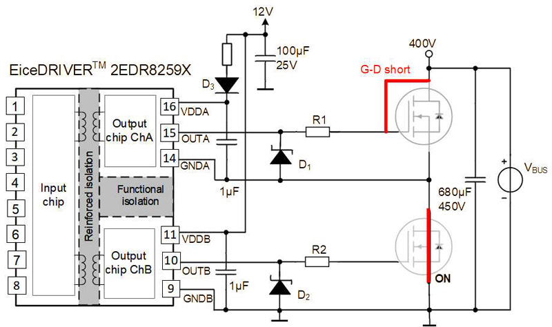
This statement is especially important when it comes to safeguarding individuals against electric shocks. Imagine this worst-case scenario in a half-bridge topology: The high-side MOSFET has a gate-drain short while the low-side MOSFET is conducting. In such an electrical overstress (EOS) event, currents higher than 600 A can surge towards the gate driver IC output.
To protect the gate driver IC output, the gate resistor (R1) is often complemented with a suppressor diode (D1), as shown in Figure 1.
The suppressor diode bypasses the gate driver output, directing the excess current to the half-bridge’s midpoint. This design ensures the gate driver IC’s isolation barrier between its output and input sides remains intact, assuming a proper application design is chosen.
Furthermore, the package integrity must be maintained during such EOS events. This means no bare metal, typically covered by mold, is exposed. EOS experiments have shown that gate driver ICs with the isolation barrier embedded on its inputs side, such as Infineon’s EiceDRIVER™, meet both of these requirements, even without the external suppressor diode (D1).
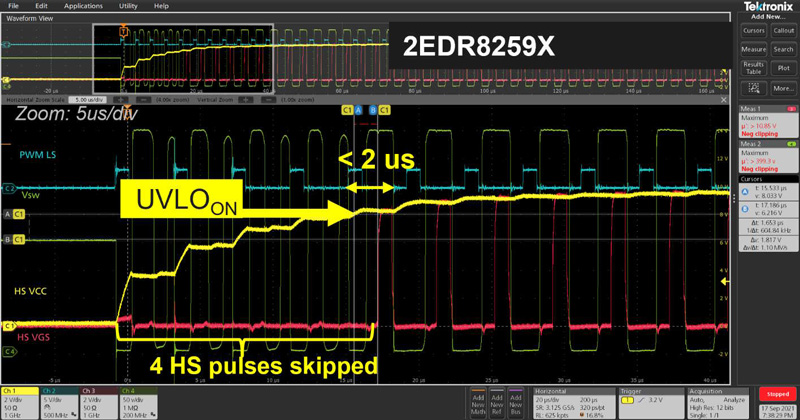
Short output stage UVLO startup time
Bootstrap supply of power supplies is common, because it is a cost-effective solution for high-side gate driver ICs. Hence, bootstrap circuits are prevalent in half- and full-bridges in high-voltage LLCs (typically with a 400 V DC bus voltage) or hard-switching full-bridges on the primary side of low-voltage DC-DC converters (48 V to 12 V).
Designs that employ bootstrap circuits benefit significantly from short gate driver IC UVLO startup times in several ways:
a. Enables faster overall system startup
b. Enables rapid recovery from brown-outs — faster LLC startup after a brownout lasting longer than 200 ms (typically equating 10 mains cycles)
c. Facilitates quick LLC startup when a restart release is initiated after the activation of system-level protection
d. Prevents main power transformer saturation due to asymmetric high-side vs low-side PWM operation during the ramp up of the bootstrap supply
For instance, using dual-channel galvanically isolated gate driver ICs with a typical UVLO startup time of 2 µs in a bootstrapped high-side configuration results in skipping only about four high-side pulses until the half-bridge can start operating (assuming a typical VDD rise rate on the high-side). In contrast, a similar gate driver IC with a UVLO startup time of 10 µs or higher can easily lead to skipping ten or more high-side pulses. This significantly delays starting the half-bridge operation, as shown in Figure 2.
Click image to enlarge
Figure 2: UVLO startup time
Optimized UVLO shutdown delay
When it comes to UVLO-triggered output-stage shutdown, the idea is to be fast enough to protect the switching device from thermal overload; but it cannot be too fast. If only a brief drop occurs below the UVLOoff threshold—caused by a sudden load jump—the switching stage should not be turned off, as it can disrupt system operation. Practical experience shows that a shutdown delay of 500 ns provides a good balance to avoid noise or ringing on VDD due to load jumps while still providing timely protection.
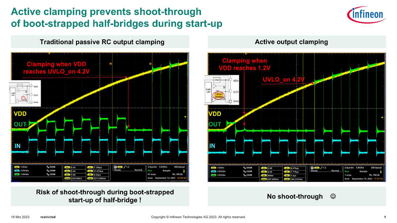
Active output clamping
Active output clamping ensures that the output stage remains safely off during system startup as long as the gate driver supply is below the UVLOon threshold. This reduces the risk of shoot-through during bootstrapped startup of half-bridges. When the supply exceeds the UVLOon threshold, the gate driver IC output stage is expected to operate according to the control input status, meaning that the output clamping is disengaged and follows the input signal.
In a bootstrapped half-bridge, when the low-side switches to charge the boost capacitor, a capacitive voltage divider (consisting of CGD and CGS of the high-side switch) causes VGS to rise above its on-threshold. The gate driver IC output clamping prevents this VGS rise by short circuiting this. In case the output clamping is not provided, the high-side switch turns on simultaneously with the low-side, creating a damaging half-bridge shoot-through.
Advanced gate driver ICs have an output clamping circuit that becomes active at VDD levels as low as 1.2 V—perfect for a “textbook-perfect” startup sequence for the high-side switch, as shown in Figure 3.
Click image to enlarge
Figure 3: Active clamping prevents shoot-through
In contrast, gate driver ICs with slow internal RC clamping circuits cause a certain level of shoot-through during half-bridge startup, until VDD rises sufficiently to activate output clamping. This leads to electrical overstress for the switching devices.
Propagation delay accuracy
While input-to-output propagation delay is an initial consideration, propagation delay accuracy across the operational temperature range, including part-to-part variations, is far more critical. The better this accuracy, i.e. the shorter the time, the less slag time is needed to accommodate this tolerance.
In practice, a good propagation delay accuracy translates into minimized dead-time losses, further improving efficiency. This becomes more important as the switching frequency of an SMPS stage rises. Modern isolated gate driver ICs achieve a typical accuracy of ±2 ns and a minimum accuracy of ±4 ns.
Shoot-through protection with configurable dead-time
In half-bridges, dead-time is introduced between turning one switch off and the other one on. This lets the switch’s tail current decay, preventing shoot-through. For superjunction power MOSFETs, like Infineon’s CoolMOS™, typical tail current decay time is around 300 ns.
In a properly working system, the controller IC manages the dead-time via software. This way, the controller IC manages the effective duty cycle of that switching stage. The software-controlled effective dead-time is a factor of the real-time hardware performance, the operating system, and the application software. Consequently, effective dead-times are rarely shorter than 300 ns—and are often significantly longer.
To hedge against cases of malfunction in software-based dead-time control, the shoot-through and dead-time control built into the gate driver IC serve as a second-level safety mechanism to prevent shoot-through. Modern dual-channel isolated gate driver ICs offer a configurable dead-time setting through an external resistor. This lets you select dead-times ranging from 100 ns to 1000 ns, making these ICs very versatile for a wide range of power-switch technologies. The accuracy of this hardware-enforced dead-time is typically way better than software-based control.
Package innovations
· Compact leadless packages: When it comes to dual-channel galvanically isolated gate driver ICs, the package size is a vital consideration. Designers can now opt for leadless 4x4 mm2 package options for these ICs instead of their larger 5x5 mm² counterparts. This reduces the PCB footprint of the gate driver IC by 36%. These packages can still offer substantial input-to-output isolation ratings, e.g., VISO of 2250 VRMS (UL 1577)
· Thermal pads: For applications where an absolute maximum input-to-output isolation voltage of 1500 Vrms is sufficient, designs incorporating exposed pads on the bottom side of the package significantly improves thermal resistance. This can bring down RthJB to as low as ~10 K/W, improving the thermal margin at the application level.
· Optimal pin configuration: Dual-channel galvanically isolated gate driver ICs in 150 and 300 mil DSO packages are increasingly offered in 14-pin configurations instead of the traditional 16-pin ones. This is achieved by removing the former “no connect” pins on the output side. This opens up additional PCB top-level routing options.
Additionally, the resulting channel-to-channel creepage distance is increased to 3.3 mm. This allows a channel-to-channel functional isolation voltage of up to 1025 VRMS (according to IEC 60664-1 Pollution class I)
· Minimal input pins: While most modern dual-channel non-isolated gate driver ICs feature two enable inputs, these inputs are frequently tied to a fixed potential, rendering them unused. For high-power-density designs where every millimeter counts, removing these redundant inputs can be both space- and cost-effective.
Dual-channel non-isolated gate driver ICs with 6-pin packages, such as the leaded SOT-23 or leadless ultra-small 1.1x1.5 mm2 6-pin TSNP packages retains all core gate driver IC features—digital on/off behavior, defined UVLO, 5 A strong output stages, and single digit ns propagation delay accuracy—while minimizing PCB area consumption and improving the PCB layout flexibility.