All Semiconductor Switch Technologies Lead to Rome
Over the past years, the industry has converged on a collection of switching topologies
Much is made of wide bandgap technologies, especially since GaN and SiC often have a superior performance on paper when compared to classic Si switching devices. These improvements include lower on-resistance and higher thermal conductivity, features that enable improvements in efficiency and operation at higher temperatures in the end application. In the context of switching power supplies (SMPS) this can mean improved system efficiencies and higher power densities. However, these improvements require more than just replacing Si devices with wide bandgap alternatives. And, of course, there will be cases where Si actually remains the optimal technology choice.
High-Performance SMPS Design
Over the past years, the industry has converged on a collection of switching topologies
This applies both to the power-factor correction (PFC) stage and the isolated high-voltage DC/DC (HV DC/DC) converter. One of the starting points is to perform side-by-side comparisons of the different switch technologies to see whether GaN or SiC deliver benefits over Si solutions.
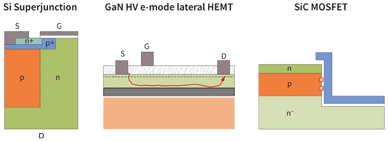
The first point to note is that both Si superjunction and SiC MOSFETs have a similar, vertical structure, whereas GaN MOSFETs employ a lateral approach. This means that in Si and SiC devices current flows from the top to the backside substrate through the device. The lateral approach of GaN means that current flows across the device with the source, gate and drain connected to the surface via separate metallisation layers (figure 1). This essentially undoped, low-impurity crystal structure enables a high mobility of electrons, hence their name: high-mobility electron transistors (HEMT).
This difference in construction, coupled with the differing semiconductor material used, leads to contrasting performance characteristics. These are often viewed in terms of figures of merit (FoM) that combine their conduction (RDS(ON)) and switching losses in order to enable side-by-side comparisons.
Click image to enlarge
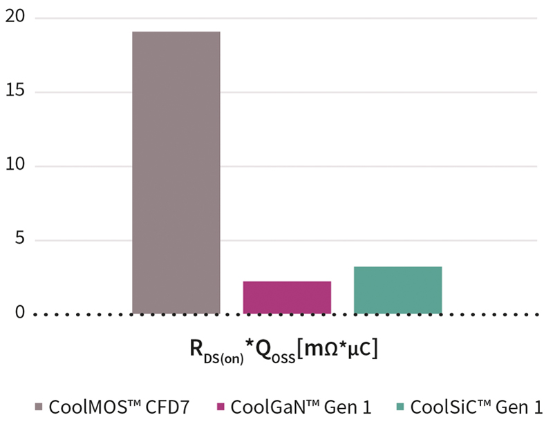
Figure: 2a: Figures of Merit for 600 V/650 V-rated switches in the differing semiconductor technologies
Click image to enlarge
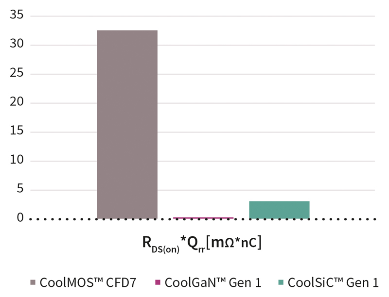
Figure 2b: Figures of Merit for 600 V/650 V-rated switches in the differing semiconductor technologies
Click image to enlarge
Figure 2c: Figures of Merit for 600 V/650 V-rated switches in the differing semiconductor technologies
Click image to enlarge
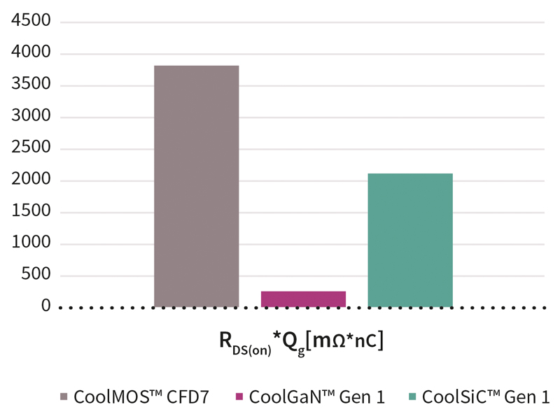
Figure 2d: Figures of Merit for 600 V/650 V-rated switches in the differing semiconductor technologies
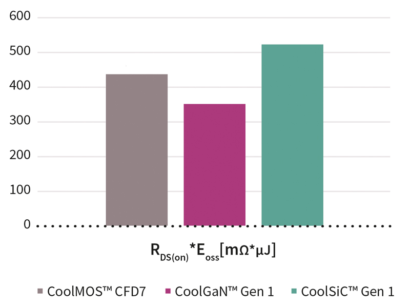
Considered in terms of drain-source charge (Qoss), recovery charge (Qrr) and gate charge (Qg), SiC MOSFETs have a better FoM than competing Si superjunction devices. However, when it comes to the energy stored in the output capacitance (Eoss), Si devices have the upper hand. In comparison, GaN MOSFETs appear to only deliver benefits when compared to the alternatives. However, it is necessary to dig a little deeper in order to appreciate the bigger picture.
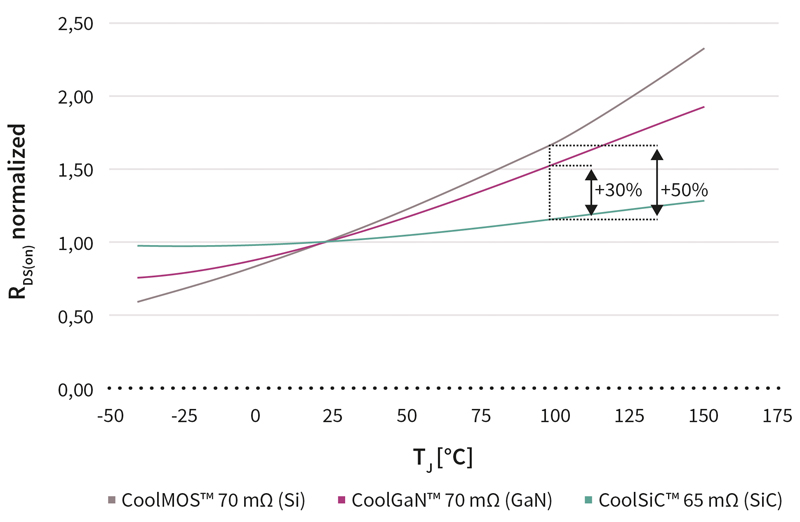
SMPS are increasingly expected to deliver higher quantities of power in ever decreasing volumes of space. This reduction in space between components inevitably leads to higher operational temperatures, a factor that impacts RDS(ON). Thanks to the low impurity level in GaN HEMTs, RDS(ON) shows a lower temperature dependency than Si devices. However, it is SiC devices that show the least RDS(ON) dependency on temperature. Normalising the values at 25°C, the RDS(ON)of SiC devices can lie 30% below GaN HEMT and 50% below Si superjunction devices at 100°C (figure 3). This implies that a Si superjunction device with an RDS(ON)of 70 mΩ could have a worse FoM than a 100 mΩ SiC device at system operating temperature, something that will impact overall efficiency of the SMPS.
Click image to enlarge
Figure 3: Normalised RDS(ON)for Si, SiC and GaN at various junction temperatures TJ in °C
Case Study: 3 kW Telecoms SMPS
Always-on applications that power services, such as telecoms power supplies, are continuously looking for ways to improve operating costs. Today, 97% efficiency is considered standard while 98% is considered a premium product. Design engineers are challenged with finding the optimal topology and choice of semiconductors so that, in combination, both the PFC and HV DC/DC stages deliver the system efficiency desired.
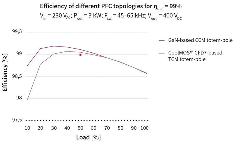
A 48 Vout, 3 kW telecoms SMPS that need to attain a ηpeakof 98% at 50% load will need to target 99% efficiency in the PFC stage. Typical approaches will utilise totem-pole topologies, either full or half-bridge in continuous conduction mode (CCM) or triangular current mode (TCM), dual-boost, or an H4/H-bridge. However, not every semiconductor technology is an ideal fit when trying to attain the highest level of efficiency. Of particular note is the use of GaN devices in a full-bridge CCM totem-pole which, at 99.3% efficiency, just edges ahead of the >99% attained with an Si superjunction MOSFET in a TCM totem-pole design (figure 4).
Click image to enlarge
Figure 4: Efficiency of totem-pole PFCs designs based upon GaN and traditional Si devices can attain >90% efficiency
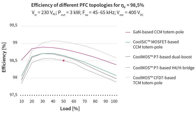
However, the new GaN and SiC semiconductor technologies do not perform as well in other topologies. A GaN-based CCM half-bridge totem pole saves two switches, but at ~98.8% efficiency it is not suitable for an SMPS targeting efficiencies of 98%. The same applies when using SiC switches in a CCM totem-pole topology, attaining around 98.6% efficiency (figure 5). This demonstrates that, despite their excellent paper-based performance, superjunction Si MOSFETs can still outperform these new technologies in topologies that allow them to operate to their strengths. Of course, it must also be noted that the TCM Totem Pole PFC topology that they were used in is the most expensive approach of those compared and most complex in terms of control.
Click image to enlarge
Figure 5: Traditional Si switches, in topologies that play to their strengths, can outperform both GaN and SiC-based PFC alternatives
This leads us to a critical point of learning: silicon switches currently continue to offer a price advantage at the component level, and design engineers can still utilise their considerable design experience with this technology. However, designers should not underestimate the complexity, in both design and control, these Si-based PFC topologies need to attain the efficiencies that wide bandgap devices can achieve with, by comparison, less effort.
The next step is to review the HV DC/DC stage. Again, the goal is to attain the highest possible efficiency in order that the overall goal of 98% at 50% load can be fulfilled, meaning this stage needs to achieve a minimum 99.1% efficiency at 50% load. A half-bridge LLC is perhaps the simplest topology to use, being well understood by designers, and lends itself for use with Si, GaN and SiC. However, it is typically limited by its inability to deliver SMPS peak efficiencies above 97% (50% load), which also depends on the performance of the PFC at the same load condition.
Attaining 98% SMPS peak efficiency at 50% load with sufficient margin is definitely possible with a three-phase interleaved half-bridge LLC, but here there is no need to use GaN and SiC switches as they will not deliver any additional benefits. There are also some design density advantages to be had here through the integration of the three transformers onto a single core. However, this is not a simple task and demands some significant capability in the analysis of magnetics.
If GaN or SiC devices provide other advantages, such as in their packaging options, then a dual-phased interleaved full-bridge or half-bridge LLC topology is suitable for wide bandgap use. Both approaches, thanks to their interleaving, spread the heat generated across the entire circuit. The half-bridge benefits from a lower component count and simpler control approach, while the full-bridge offers better ripple control and a slightly better heat spread.
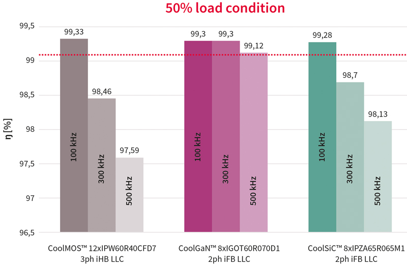
Of course, power density, if it is also a critical aspect of the design requirements, needs the HV DC/DC stage to operate at a higher switching frequency to bring down the size of the magnetic components. This comes at the price of a loss of efficiency, but the loss varies between Si, GaN and SiC. Si is most adversely impacted as the LLC resonant frequency moves to 300 kHz and then 500 kHz, with less impact on SiC. GaN technology, however, shines through with impressive performance even at 500 kHz (figure 6).
Click image to enlarge
Figure 6: Impact of resonant frequency on LLC topology’s efficiency for Si, GaN and SiC
The resulting power density improvement then depend on where the volume can ultimately be saved. SMDs, miscellaneous components, and the auxiliary power supply have little impact. Volume savings are mostly to be found in the transformers and inductors, electrolytic capacitors, power semiconductors, and heatsinks and cooling implementation. All in all, the potential volume saving will be capped at around 30% for a move from 100 kHz to 300 kHz resonant frequency.
So, Which Technology is Better?
It should be clear that clarity is not to be found simply by choosing the switching technology that offers the best FoM. Traditional Si switches, around which enormous amounts of design and implementation experience is available in the industry, will continue to play at the top table in the most demanding of SMPS designs, quite simply because they deliver the best efficiency in some cases. However, wide bandgap technologies, such as GaN and SiC, can deliver advantages in appropriate topologies and when specific design targets, such as power density (GaN) or operation in harsh and high-temperature environments (SiC), must be attained. The analyses undertaken here underscore the importance of the balanced and open-minded approach needed, in combination with a trusted supplier, when selecting semiconductor switches without giving way to the distraction of shiny advanced technologies that appear attractive simply because they are the newest tool on the shelf.
Infineon Technologies AG