Gallium Nitride (GaN) devices have silicon-like electrical properties and can be driven by many off-the-shelf driver products used in silicon MOSFET designs.
Figure 1. GaN transistors enable more efficient, cooler-running, compact, and cost-efficient designs
GaN offers low RDSon/VDSon, high electron mobility, and other characteristics that result in more efficient designs. Higher switching frequencies allow designers to make tradeoffs between efficiency and switching speed for application-optimized designs. These characteristics enable more efficient solutions, run cooler, are four times smaller, and cost 10%-20% less than an equivalent Si-based design (Figure 1).
GaN’s sweet spot is applications with operating voltages between 48 V and 600 V, making it well-suited to offer more compact, cooler-running, and cost-effective alternatives to Si-based MOSFETs.
GaN Drive Requirements
GaN’s electrical properties differ from silicon devices. They have low gate-to-drain capacitance and start to conduct significant current at 1.6 V, so care must be taken to ensure a low impedance gate-to-source path when the device needs to be held off during high-speed switching in a rectifier function.
Paradoxically, the switching speed of these devices can be too fast, which can cause ringing and injection of unwanted high frequencies into the circuit they are driving. Their high dV/dt can reduce efficiency by creating shoot-through during the “hard” switching transition. Fortunately, this can be controlled. The industry has developed several approaches to “normalize” GaN device drive characteristics:
Enhancement-Mode Gate Injection Transistor (GIT): Adding a p-doped gate to aGaN- GIT causes it to function as a normally-off device (Figure 2). This allows precise control of on/off switching speed and can be connected in parallel to support higher current applications. On the negative side, they require a special drive circuit with very high gate current requirements that reduce efficiency.
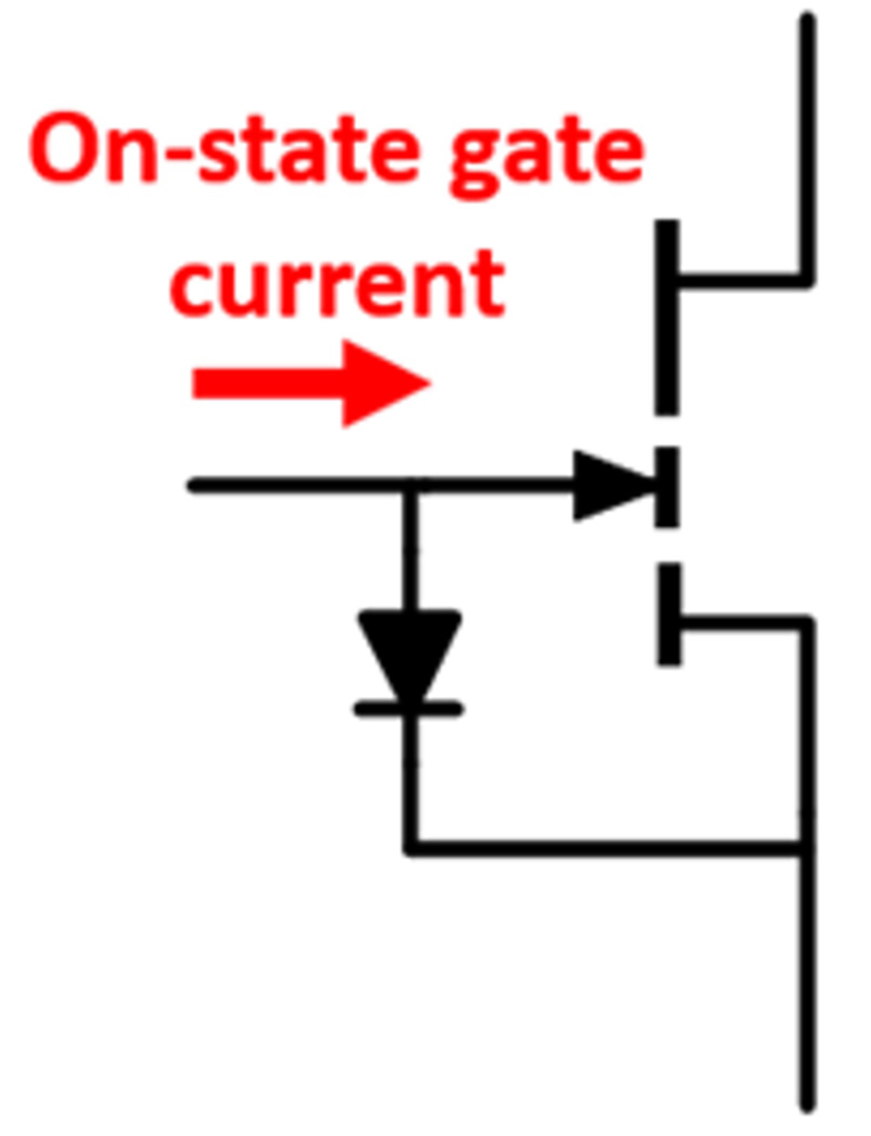
Click image to enlarge
Figure 2. Enhancement Mode GIT
Cascode GaN: This approach creates a stacked die cascode by co-packaging a naturally “off” low-voltage, low RDSon silicon MOSFET placed in series with the depletion-mode GaN HEMT transistor (Figure 3). This composite device can be driven by the same gate drivers used for silicon power devices but has drawbacks. For example, performance is limited by the silicon MOSFET’s reverse recovery and avalanche characteristics, and no way to adjust its on/off switching speed. It can be challenging to configure for parallel operation and requires external noise damping, typically a ferrite bead.
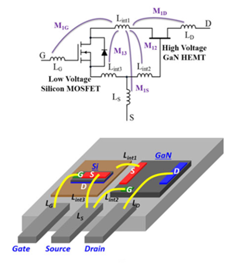
Click image to enlarge
Figure 3. A GaN transistor co-packaged with a silicon MOSFET in cascode configuration
Depletion Mode Device with a Co-Packaged Driver: Several companies have made depletion-mode GaN devices easier to use by co-packaging them with a custom silicon driver that allows the device to mimic characteristics of a conventional silicon power MOSFET. This makes it possible to integrate over-current and over-temperature protection within the package, saving space and cost. But advantages come at the cost of design flexibility because the drive values cannot be optimized for a particular application. Additionally, the external driver only allows adjustment of the switch’s turn-on time and makes paralleling difficult.
Monolithic GaN + Integrated Driver: This approach integrates the GaN power device and companion driver circuit on the same substrate. The on-chip driver can be designed to provide near-ideal signal levels to the power transistor’s gate while presenting a “silicon-friendly” interface that works with most MOSFET driver devices and reduces internal parasitics. While this simplifies design, it requires external passive components to implement a functional solution. The on-chip driver is simple with no OTP/OCP or other protection circuitry. And like devices with co-packaged drivers, only their switch-on rise time can be controlled and are difficult to configure for parallel operation.
Enhancement-Mode (E-mode) GaN
E-mode GaN solves many problems associated with earlier GaN-based power devices. This approach is based on a HEMT structure that forms an intrinsic E-mode device that is voltage driven and normally off.
A discrete E-mode GaN power device has electrical characteristics similar to silicon MOSFETs familiar to designers, including:
· Compatibility with many silicon MOSFET drivers.
· Design flexibility comparable to discrete silicon MOSFETs.
· Switching slew rates (on and off) that can be optimized by adjusting gate resistance (RG).
· Ease of configuration for parallel operation.
· Silicon-like characteristics allowing the use of common techniques for designing and testing applications.
These are the most common methods to drive GaN devices. As GaN devices do not behave precisely like silicon, considerations must be taken with each approach.
GaN Systems has built on these intrinsic properties to create advanced E-mode products with robust device structures that exceed AEC-Q101 and JEDEC reliability standards and complaint with JC-70 and FIT standards. Features such as a robust gate structure that accepts an input range of -20 V/+10 V that can work with unipolar (0 V/+6 V) and bipolar drive levels (-3 V/+6 V and -6 V/+6 V) while providing robust operational margins make these products compatible with many commercially available driver ICs used for MOSFET-based designs in bridges, power converters, and other power applications.
Although modern E-mode GaN devices are much simpler to work with, they have several unique characteristics unlike their silicon counterparts:
· QG lower than comparable silicon devices, providing lower drive losses and faster switching speeds.
· Higher gains and lower VGS in power transistors typically requiring a +5 V/+6 V gate bias to turn on.
· A lower gate threshold voltage VG(th), typically 1.5 V.
Driving E-Mode GaN Transistors
Take a look at the practical implications of the E-mode GaN device’s unique properties regarding selecting and fine-tuning a gate driver circuit for real-world applications. The primary design goals of an E-mode GaN device driver:
· Provide the switch with the correct turn-on/turn-off waveforms with the desired voltages (RDS(on) and IDS(max) is a function of VGS).
· Maximize switching performance by:
o Feeding the GaN FET with reliable, clean switching waveforms.
o Providing a clean gate source and sink currents (IGS).
· Control power devices’ slew rate to reduce EMC (the GaN FET’s di/dt, dv/dt can be controlled by varying RG).
· Enable precise dead time control to minimize switching losses.
· Drive voltage considerations.
GaN Systems E-mode transistors can be run with a positive-only VGS driver that delivers VGS(OFF) = 0 V/VGS(on) = 6 V, making them a great choice for low-voltage or low-power applications or where minimizing dead time loss is critical.
Drive configurations that provide a negative VGS(OFF) are preferred when high noise immunity and reduced switching losses are a priority. A symmetrical +/- 6 V or a +6 V/-3 V drive input can be used.
System Trade-Offs Using the Influence of Negative Drive Voltage
Applying a negative VDR(OFF) reduces the energy required to turn off an E-mode GaN transistor, which becomes more apparent as operating current increases. A non-negative drive signal can be used for lower-power applications without incurring significant switching losses, but that switching the gate off with a negative VDR(OFF) becomes essential for high-current applications. Applying negative VDR(OFF) makes the power stage more efficient under higher power, but it must be used in conjunction with precise dead time control to achieve optimum system efficiency.
Managing Dead Time Losses in GaN Devices
GaN HEMTS do not have a body diode. The device’s reverse conduction voltage drop increases proportionally to VGS(OFF). During dead time, 2DEG behaves like a diodewith VF = VTH(GD)+ VGS(OFF)+ ISD* RSD(ON).
These phenomena cause dead time losses to increase as VGS(OFF) increases. If the drive signal’s dead time falls below a certain threshold, the device will not be at zero volts during part of the time it is switching, and the energy in the switching circuit’s capacitors will be dissipated in the channel.
The device’s losses increase sharply as the zero-voltage switching (ZVS) period decreases. As a result, a designer must derive a dead time that is long enough to prevent ZVS losses and short enough to keep the GaN device running efficiently.
Switching Speed Control with External RG
GaN devices can switch so rapidly that the sharp rising and falling edges of their output waveform (dv/dt) can generate unwanted high-amplitude harmonics, which create EMI issues. As with MOSFETs, E-mode GaN transistor switching speed (both on and off) can be controlled by adjusting the resistance placed in series with the device’s gate (RG). This technique is valuable for system EMCoptimization. Other GaN implementations such as integrated driver and cascode configurations isolate that gate, thereby limiting RG switching speed control to the turn-on part of the cycle or making it impossible.
Gate Drive Considerations for Paralleling
Parallel operation of GaN Systems E-mode devices is straightforward, but interaction between the gates of the paralleled devices, or gate ringing, must be prevented by adding distributed gate resistors (R3/R5 = 1-2Ω) and source resistors (R6/R7 = 1-2Ω).
These guidelines were verified in an experiment where four GaN Systems GS6651T devices were run in a parallel configuration with four paralleled GS6651Ts running in freewheel mode on the other side of the bridge circuit.
For these tests, gate resistance was set at RG_ON=4.55 Ω, RG_OFF = 1.25 Ω. The test circuit’s supply voltage (VBUS) was 400 V with gate drive input (VGS) = +6.8 V/-5 V. The circuit produced a clean waveform as it was hard switched from its idle state to the full rated current measured drive currents (IDS_ON=231 A, IDS_OFF=240 A with ~200 V VDS margin).
Conclusion
E-mode GaN transistors offer high efficiency and performance along with silicon-friendly electrical characteristics that make it easy to incorporate them in various applications using many of the same drivers used for MOSFET-based designs.