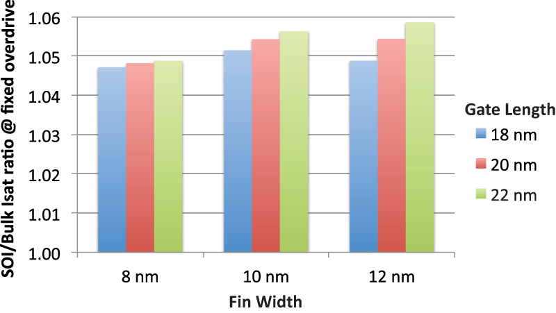
Arguing the FinFET ideal shape for performance
The triangular shape of the Intel bulk FinFETs and its implications for the transistor performance, compared to ‘ideal' rectangular-shaped transistors has as its main observations noted a worsening of the short channel effects, and a reduction in the on-current by 12-15% compared to rectangular-gate bulk FinFETs. (Gold Standard Simulation) GSS CEO, Asen Asenov, has implied that SOI FinFETs with an almost ideal rectangular shape may be a better design for future FinFET scaling. The resulting question is being asked is ‘assuming that you can make ideal rectangular bulk and SOI FinFETs, which one will have better performance?'
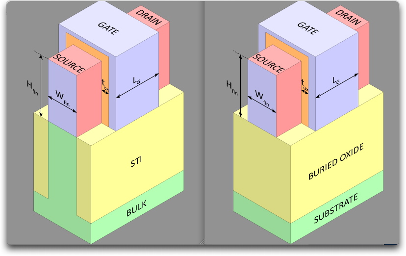
GSS provides some answers, assuming bulk and SOI FinFET designs illustrated schematically in Fig. 1 with exactly the same geometry of the fin and with undoped channels. The nominal device dimensions are LG=20 nm, Wfin=10 nm and Hfin=25 nm. The main difference between the two devices is the presence of a stopper beneath the channel in the bulk FinFET case, which prevents DIBL (drain-induced barrier lowering) and improves the short-channel effects of the bulk FinFET. The presence of the SOI substrate eliminates the need for such a stopper in the case of the SOI FinFET.
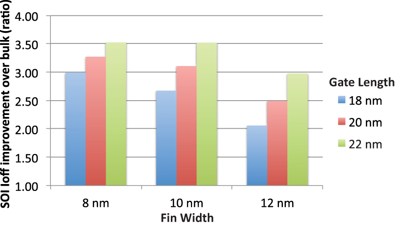
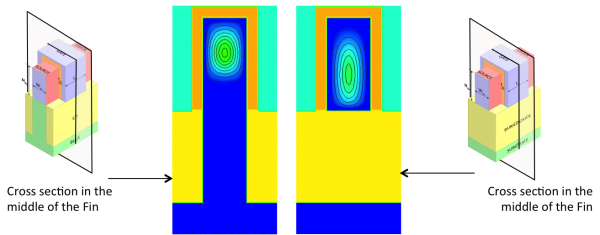
Fig. 4 provides the physical explanation for these findings. The necessary presence of the stopper below the channel in the bulk fin leads to the carriers being pushed up towards the top of the fin (due to the built-in potential between the undoped channel and the highly-doped stopper), reducing the effective channel width and somewhat reducing the FinFET performance for the same physical fin height.
The detailed design of the 20nm channel length FinFETs simulated in this blog as well as the optimal design of 14nm and 10nm bulk and SOI FinFETs are described in GSS report. Gold Standard Simulations