Measuring SiC Schottky Diode Ruggedness with A High Voltage Pulse Generator
In Part 1 of this discussion, we explored the functionality of a series-connected avalanche transistor pulser, specifically for the purpose of evaluating dV/dt ruggedness of SiC Schottky diodes. In this issue, the diodes are tested with the new pulser design.
SiC Schottky diode dV/dt ruggedness testing
With a verified high-speed pulser in place, Cree conducted a series of dV/dt ruggedness tests on a 600V 3A Schottky diode*. The intent of the tests was to use the new setup to exercise the diode with an extremely fast pulse to determine the eventual dV/dt limitation. This would give improved indication of the dV/dt ruggedness of the entire family of diodes with identical design rules.
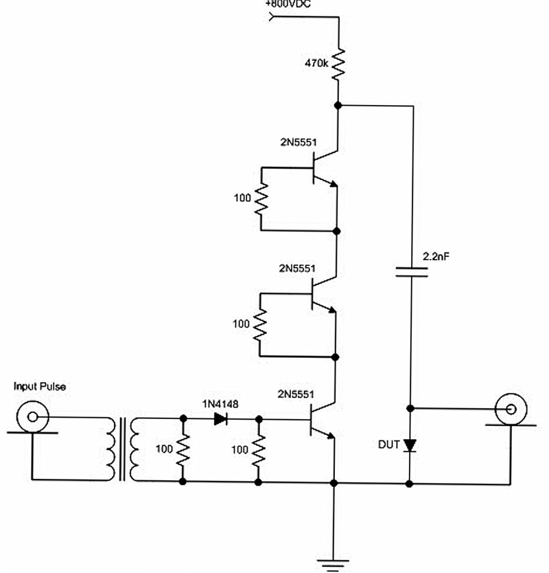
The series-string avalanche pulser was equipped with 2N5551 silicon bipolar transistors (max VCEO=160V) in order to achieve higher transition voltages, and the 200Ω resistor (RLOAD) was replaced with the diode, or DUT (device under test). The test pulse for the diode was set to 800V. A schematic of the test setup is shown in Figure 1, and the results of the test are shown in Figure 2.
Click image to enlarge
Figure 1: Schematic for the 600V, 3A Schottky diode* dV/dt ruggedness test setup
Click image to enlarge
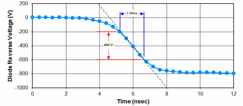
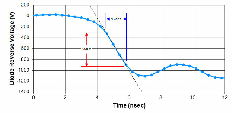
Figure 2: 600V, 3A Schottky diode* reverse dV/dt = 295 V/ns
The measured reverse (turn-off) dV/dt was 295V/ns, or about six times faster than the typically reported 600V diode dV/dt ruggedness specification of 50V/ns [14]. It is also roughly three times greater than the previous measurements obtained in earlier testing by Cree. As before, no device failures were encountered during the course of these tests, clearly demonstrating the enhanced dV/dt ruggedness of this SiC diode, as well as providing a clear indication of the ruggedness of this particular family of SiC Schottky diodes. While further testing of additional devices is required for final confirmation, these results indicate that the dV/dt ruggedness of this Schottky diode family exceeds 300V/ns.
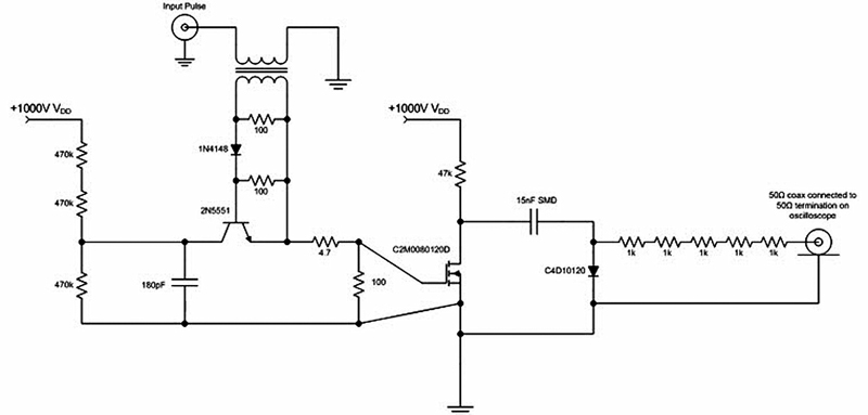
The logical next step was to perform the same testing on a higher voltage family of diodes to gain an indication of the dV/dt ruggedness at the higher rated voltages. The DUT for these tests was a 1200V 10A SiC diode**. The schematic of the test setup is shown in Figure 3, with the applied voltage (VDD) set to 1000V. Note that the pulse generator circuit required modification to account for VDD and the rated VRRM of 1200V of the higher voltage Schottky diode being tested.
Click image to enlarge
Figure 3: Schematic for the 1200V 10A SiC Schottky diode** dV/dt ruggedness test setup
Two of the 2N5551 silicon transistors have been replaced by a single 1200V SiC MOSFET***. The SiC MOSFET is turned on quickly via a pulse applied to the remaining 2N5551 avalanche transistor. The activation of the SiC MOSFET causes the top terminal of the SMD capacitor to discharge to ground, resulting in a reverse bias pulse of 1000V to be applied to the DUT. The voltage was measured with the low impedance resistive divider to minimize ringing.
As shown in Figure 4, the measured reverse dV/dt was 490 V/ns, or approximately six times faster than the typically reported diode dV/dt ruggedness value of 80V/ns of 1.2kV SiC JBS diodes [16]. No device failures were encountered during the course of these tests, which clearly demonstrates the dV/dt ruggedness of this higher voltage SiC diode and provides a clear indication of the ruggedness of the entire device family.
Click image to enlarge
Figure 4: 1200V 10A SiC Schottky diode** reverse dV/dt = 490 V/ns
Conclusions
The dV/dt ruggedness of SiC Schottky diodes can be still a concern for many designers. The goal of this work was to design a pulser capable of subjecting the test devices to a dV/dt significantly faster than what would be experienced in practice, in order to further characterize the 600V and 1200V SiC Schottky diodes that are increasingly employed in modern high-voltage power-conversion systems.
Furthermore, the Wolfspeed diodes tested demonstrated six times higher dV/dt ruggedness than what is typically reported in the industry, with values of 295V/ns and 490V/ns, respectively. Most importantly, no failures were observed with any of the devices tested, which means the actual limits of these diodes exceeds these values. As of this writing, the ultimate dV/dt ruggedness of these devices remains unknown.
*Part I was published November 5, 2015
Footnotes
*Cree C3D03060A
** Cree C4D10120A
*** Cree C2M0080120D
BIBILOGRAPHY
[1] S. Hodge Jr., “SiC Schottky Diodes in Power Factor Correction,” Power Electronics Technology, pp14-18, August 2004.
[2] CPWR-RS01, “SiC Zero Recovery Schottky Diode Reliability at Extremely High Voltage Slew Rates”, Rev. A, www.cree.com/~/media/Files/Cree/Power/Reliability/CPWRRS01.pdf
[3] T. Barbieri, “Understanding the Design, Performance, and Dependability Differences in Today’s SiC Schottky Diodes,” How2Power, August 2015. www.how2power.com/pdf_view.php?url=/newsletters/1508/articles/H2PToday1508_design_Cree.pdf
[4] C. P. Hancock, A. R. Owens and K. O’Grady, “Simple voltage generator for producing well-defined nanosecond pulses of amplitudes in excess of 1kV,” IEE Proceedings on Measurement and Technology,” vol. 144, issue 5, pp. 229-233, 1997.
[5] W. M. Henerbry “Avalanche transistor circuits,” Review of Scientific Instruments, vol. 32, issue 11, pp 1198-1203, November 1961.
[6] T. H. O’Dell, “Series operation of avalanche transistors,” Electronics Letters, vol. 5, issue 5, pp. 94-95, 1969.
[7] E. F. Taylor, “Solid-state 1.0kV nanosecond pulse generator,” IEE Journal on Electronics Circuits and Systems, vol. 1, no. 1, pp 42-48, September 1976.
[8] D. M. Benzel and M. D. Pocha, “1000-V 300-psec Pulse generation circuit using silicon avalanche transistors,” Review of Scientific Instruments, vol. 56, issue 7, pp 1456-1458 July 1985.
[9] R. J. Baker, “High voltage pulse generation using current mode second breakdown in a bipolar junction transistor,” Review of Scientific Instruments, vol. 62, issue 4, pp 1031-1036 April 1991.
[10] E.S Fulkerson and R. Booth, “Design of reliable high voltage avalanche transistor pulsers,” Twenty- First International Power Modulator Symposium, pp 101-103, 1994.
[11] A. I. Bishop and P. F. Barker, “Subnanosecond Pockels cell switching using avalanche transistors,” Review of Scientific Instruments, vol. 77, issue 4, pp 044701-044701-5, 2006.
[12] L. L. Molina, A. Mar, F. J. Zutavern, G. M. Loubriel and M. W O’Malley, “Sub-nanosecond avalanche transistor drivers for low impedance pulsed power applications,” IEEE Conference on Pulsed Power Plasma Science, pp. 178-181, 2001.
[13] R. J. Baker and M. D. Pocha, “Nanosecond switching using power MOSFETs,” Review of Scientific Instruments, vol. 61, issue 8, pp 2211-2213 August 1990.
[14] Infineon IDH05SG60C datasheet, rev 2.4, December 12, 2012. www.infineon.com/dgdl/IDH05SG60C_rev2.4.pdf?folderId=db3a30431d8a6b3c011dbeca72db281a&fileId=db3a30431f848401011ff4cebd9a531b
[15] P. R. Prince, “Paralleling avalanche transistors,” Proceedings of the IEEE, vol. 56, issue 7, pp 1456-1458 July 1985.
[16] Infineon IDW20G120C5B datasheet, rev 2.0, October 6, 2014. www.infineon.com/dgdl/Infineon-20140610_IDW20G120C5-DS-v02_00-en.pdf?folderId=5546d4694909da4801490a07012f053b&fileId=5546d461464245d3014695635f956a3f