Measuring SiC Schottky Diode Ruggedness with A High Voltage Pulse Generator
When the first generation of silicon carbide (SiC) Schottky diodes was introduced more than 10 years ago, their widespread adoption was somewhat challenged by unforeseen dV/dt limitations within certain manufacturers’ devices. In particular, devices with lower dV/dt capability were susceptible to failure from large in-rush currents.
An initial reliability study of some of these early 600V SiC Schottky diodes reported an upper dV/dt limit of 55–60V/ns (volts per nanosecond), which unfairly tarnished the reputation of SiC diodes in general [1]. Observing that their SiC Schottky diodes were not included in the initial study, researchers at Cree (now Wolfspeed, A Cree Company) performed a subsequent reliability study on their first-generation 600V SiC Schottky diode, and demonstrated that their SiC diodes could withstand a turn-on rate of 75V/ns and a turn-off rate of 100V/ns for more than 100,000 cycles without failure [2].
Industry adoption
Since that time, the power conversion industry has seen large-scale adoption of these SiC diodes into efficiency-critical applications, such as power factor correction (PFC) circuits and motor drives, due to significant performance improvements achieved through the elimination of minority carrier reverse recovery charge and the resulting switching loss associated with traditional PiN diodes.
This, in turn, has resulted in the development of several new generations of commercial SiC Schottky diodes, with each generation bringing better performance and quality [3]. However, although SiC Schottky diode technology has progressed markedly over the past decade, all but eliminating industry-wide performance concerns, it is important to note that some end-users are still concerned that the dV/dt capability of these diodes is a potential vulnerability. Thus, in order to remain competitive, SiC diode manufacturers need to devise a universally acceptable test method that enables them to report dV/dt ruggedness as a measure of SiC Schottky diode reliability.
Let’s examine the design of a high-speed, high voltage pulse generator (pulser) and how it was used to demonstrate the dV/dt ruggedness of current-generation SiC Schottky diodes. One of the first tasks was to increase the capabilities of the pulser to enable it to drive the diodes to their limits, stressing the devices at a dV/dt significantly faster than what would be experienced in most normal power conversion applications.
While the original experiments were performed using a pulser with switching times of approximately 5ns, it was necessary to develop a pulser with switching times approaching 1ns. This was achieved by employing currently available avalanche transistors in addition to state-of-the-art SiC MOSFETs. The design, construction, and test of this high-speed pulser is described herein, along with the measured dV/dt ruggedness of 600V and 1200V SiC Schottky diodes.
Application considerations
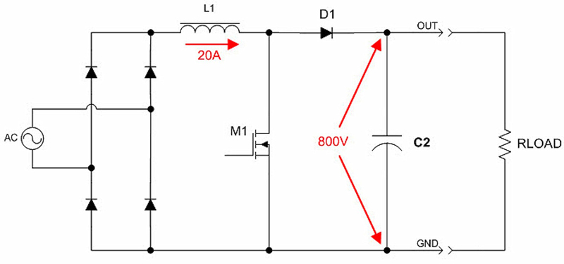
dV/dt ruggedness is one of the more significant design factors that set the limits on achievable switching speed in hard-switched applications. This can be illustrated by considering a popular application of SiC devices: the power factor correction circuit (PFC) as shown in Figure 1. The maximum switching speed of MOSFET [M1] is limited by the maximum dV/dt of the boost diode [D1]. In this example, the turn-on loss experienced by M1 is considered for the case of two diodes, each with different dV/dt limits: 50V/ns and 100V/ns.
Click image to enlarge
Figure 1: Basic PFC application
This first order analysis assumes ideal components (no parasitics) and perfectly linear switching. Initial conditions are that MOSFET M1 is off, a 20A current is flowing through L1 causing D1 to conduct, and the current flows out to the load. The voltage across C2 is 800V. When M1 turns on, D1 is rapidly reverse-biased, and the dV/dt limit on D1 (50V/ns or 100V/ns) sets the maximum turn on drain-to-source (VDS) dV/dt of the MOSFET.
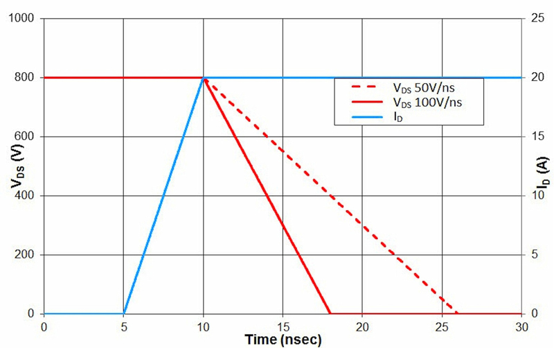
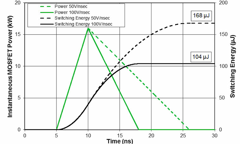
The turn-on VDS and drain current (ID) of the MOSFET for the case of each diode is illustrated in Figure 2, in which dV/dt is shown as a negative value because the voltage is falling. The current rise-time is assumed to be the same for both cases. The MOSFET’s instantaneous power (P = I*V) and switching energy (E = ∫P dt) were calculated based on these waveforms, and the results are shown in Figure 3.
Click image to enlarge
Figure 2: Ideal MOSFET turn-on waveforms for dV/dt limits of 50V/ns and 100V/ns
Click image to enlarge
Figure 3: Instantaneous power dissipation and turn-on energy loss for 50V/ns and 100V/ns
The peak instantaneous power remains the same for the two cases. Additionally, the instantaneous power is the same during the current rise of the switching event (t = 5ns to 10ns). However, the time it takes the power to drop to zero is twice as long for the 50V/ns case. Switching energy during the current rise time (5 to 10ns) is the same for both cases.
The major difference in switching energy occurs during the voltage fall time (time > 10ns). The switching energy for the 50V/ns case during this time period is twice as high as the 100V/ns case, which has a strong influence on the total switching energy. The total switching energy for the 50V/ns case is 168µJ compared to 104µJ for the 100V/ns — a 61.5% increase. Note that system switching-losses are equal to the switching frequency multiplied by the switching energy. Therefore, the significant difference in switching energy for the two cases illustrates the need for higher dV/dt ruggedness to minimize switching losses, maximize system efficiency, and enable higher switching frequencies.
Series-connected avalanche transistor pulser
The evaluation of dV/dt ruggedness requires a means of generating an extremely fast high voltage pulse. Some existing techniques include a mercury-wetted relay pulse generator [4] and avalanche transistors [5-13].
The mercury-wetted relay approach has been historically used to generate extremely fast pulses; however, a custom relay design would be required to handle the higher voltage levels necessary for this study. A second widely used approach involves operating bipolar junction transistors (BJTs) in avalanche breakdown region. This condition occurs when the BJT’s collector-to-emitter voltage (VCEO) is exceeded and the transistor enters secondary breakdown.
By limiting the time the BJT is subjected to secondary breakdown, the device can be used as an extremely fast low-jitter high-voltage switch that could be applied to characterize the dV/dt ruggedness of SiC power devices. However, the performance and reliability of commonly available BJTs is not guaranteed for repeated operation in this mode; as such, the test circuit requires an avalanche transistor type (e.g., BJTs designed specifically for avalanche mode operation). This type of avalanche transistor pulser is widely used to drive Pockels cells, streak cameras, lasers, etc., and is an excellent choice for this study. One popular configuration for a high voltage avalanche transistor pulser is the series connection generator.
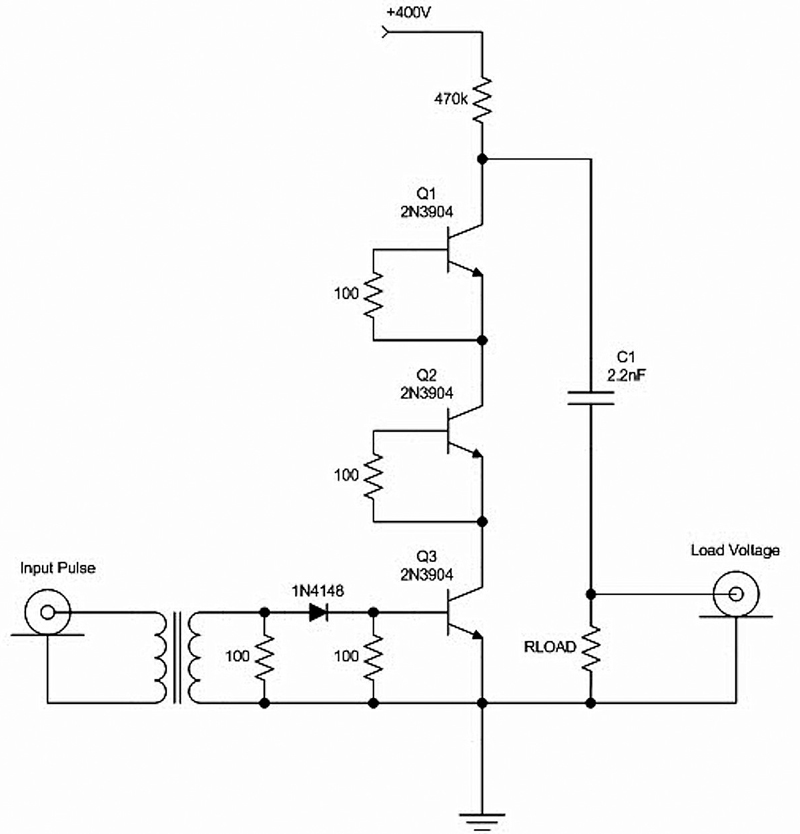
In evaluating the series-connected avalanche transistor pulser for this work, a 200Ω resistive load was used in the circuit schematic shown in Figure 4. Voltage measurements were taken with a high voltage probe connected directly to the BNC connector, with an adapter to eliminate the ground wire inductance. Waveforms were observed with a 350MHz (1ns rise time) digital sampling oscilloscope with 400MHz 100:1 probe (900psec rise time). The frequency response limitations of the oscilloscope and probe resulted in a system rise time of 1.35ns.
Click image to enlarge
Figure 4: Pulse generator using series connected avalanche transistors
The circuit places three transistors with a maximum VCEO of 40V in series. At steady state, the 400VDC input voltage is divided equally among the transistors resulting in a collector-to-emitter voltage (VCE) of 133V across each transistor, placing them close to avalanche mode. Operation of the circuit is as follows: a pulse is applied to the input and causes transistor Q3 to avalanche.
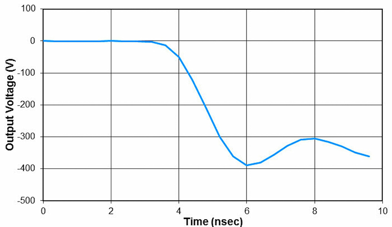
Similar to a domino effect, this action essentially causes the two remaining transistors to avalanche. This causes the top terminal of capacitor C1 to discharge to ground in less than 2ns, resulting in a high dV/dt negative-going pulse produced across the load resistor (RLOAD). The output voltage pulse is presented in Figure 5, in which the 1.35ns rise time is observed.
Click image to enlarge
Figure 5: Series connected pulse generator output terminated into 200Ω RLOAD
SiC Schottky diode dV/dt ruggedness testing
With a verified high-speed pulser in place, Cree conducted a series of dV/dt ruggedness tests on a 600V 3A Schottky diode*. The intent of the tests was to use the new setup to exercise the diode with an extremely fast pulse to determine the eventual dV/dt limitation. This would give improved indication of the dV/dt ruggedness of the entire family of diodes with identical design rules.
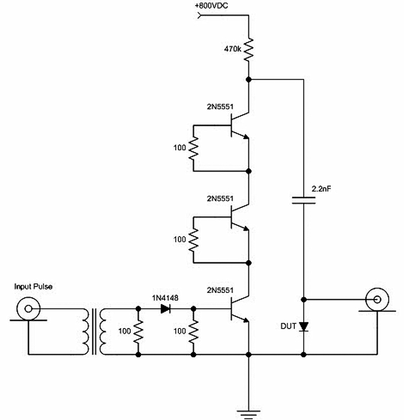
The series-string avalanche pulser was equipped with 2N5551 silicon bipolar transistors (max VCEO=160V) in order to achieve higher transition voltages, and the 200Ω resistor (RLOAD) was replaced with the diode, or DUT (device under test). The test pulse for the diode was set to 800V. A schematic of the test setup is shown in Figure 6, and the results of the test are shown in Figure 7.
Click image to enlarge
Figure 6: Schematic for the 600V, 3A Schottky diode* dV/dt ruggedness test setup
Click image to enlarge
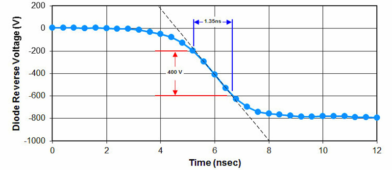
Figure 7: 600V, 3A Schottky diode* reverse dV/dt = 295 V/ns
The measured reverse (turn-off) dV/dt was 295V/ns, or about six times faster than the typically reported 600V diode dV/dt ruggedness specification of 50V/ns [14]. It is also roughly three times greater than the previous measurements obtained in earlier testing by Cree. As before, no device failures were encountered during the course of these tests, clearly demonstrating the enhanced dV/dt ruggedness of this SiC diode, as well as providing a clear indication of the ruggedness of this particular family of SiC Schottky diodes. While further testing of additional devices is required for final confirmation, these results indicate that the dV/dt ruggedness of this Schottky diode family exceeds 300V/ns.
The logical next step was to perform the same testing on a higher voltage family of diodes to gain an indication of the dV/dt ruggedness at the higher rated voltages. The DUT for these tests was a 1200V 10A SiC diode**. The schematic of the test setup is shown in Figure 8, with the applied voltage (VDD) set to 1000V. Note that the pulse generator circuit required modification to account for VDD and the rated VRRM of 1200V of the higher voltage Schottky diode being tested.

Click image to enlarge
Figure 8: Schematic for the 1200V 10A SiC Schottky diode** dV/dt ruggedness test setup
Two of the 2N5551 silicon transistors have been replaced by a single 1200V SiC MOSFET***. The SiC MOSFET is turned on quickly via a pulse applied to the remaining 2N5551 avalanche transistor. The activation of the SiC MOSFET causes the top terminal of the SMD capacitor to discharge to ground, resulting in a reverse bias pulse of 1000V to be applied to the DUT. The voltage was measured with the low impedance resistive divider to minimize ringing.
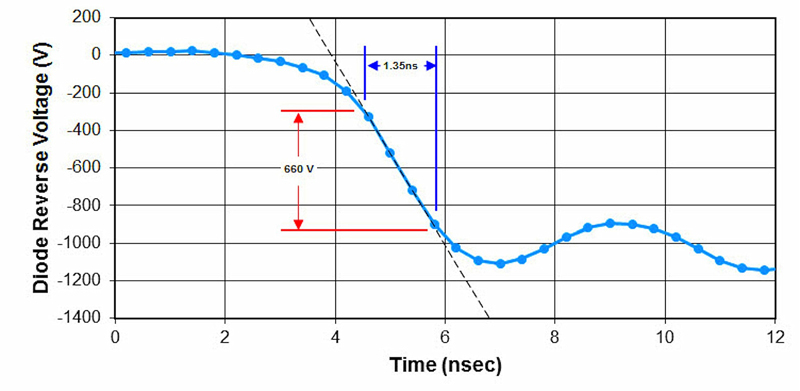
As shown in Figure 9, the measured reverse dV/dt was 490 V/ns, or approximately six times faster than the typically reported diode dV/dt ruggedness value of 80V/ns of 1.2kV SiC JBS diodes [16]. No device failures were encountered during the course of these tests, which clearly demonstrates the dV/dt ruggedness of this higher voltage SiC diode and provides a clear indication of the ruggedness of the entire device family.
Click image to enlarge
Figure 9: 1200V 10A SiC Schottky diode** reverse dV/dt = 490 V/ns
Conclusions
The dV/dt ruggedness of SiC Schottky diodes can be still a concern for many designers. The goal of this work was to design a pulser capable of subjecting the test devices to a dV/dt significantly faster than what would be experienced in practice, in order to further characterize the 600V and 1200V SiC Schottky diodes that are increasingly employed in modern high-voltage power-conversion systems.
Furthermore, the Wolfspeed diodes tested demonstrated six times higher dV/dt ruggedness than what is typically reported in the industry, with values of 295V/ns and 490V/ns, respectively. Most importantly, no failures were observed with any of the devices tested, which means the actual limits of these diodes exceeds these values. As of this writing, the ultimate dV/dt ruggedness of these devices remains unknown.
Footnotes
*Cree C3D03060A
** Cree C4D10120A
*** Cree C2M0080120D
BIBILOGRAPHY
[1] S. Hodge Jr., “SiC Schottky Diodes in Power Factor Correction,” Power Electronics Technology, pp14-18, August 2004.
[2] CPWR-RS01, “SiC Zero Recovery Schottky Diode Reliability at Extremely High Voltage Slew Rates”, Rev. A, www.cree.com/~/media/Files/Cree/Power/Reliability/CPWRRS01.pdf
[3] T. Barbieri, “Understanding the Design, Performance, and Dependability Differences in Today’s SiC Schottky Diodes,” How2Power, August 2015. www.how2power.com/pdf_view.php?url=/newsletters/1508/articles/H2PToday1508_design_Cree.pdf
[4] C. P. Hancock, A. R. Owens and K. O’Grady, “Simple voltage generator for producing well-defined nanosecond pulses of amplitudes in excess of 1kV,” IEE Proceedings on Measurement and Technology,” vol. 144, issue 5, pp. 229-233, 1997.
[5] W. M. Henerbry “Avalanche transistor circuits,” Review of Scientific Instruments, vol. 32, issue 11, pp 1198-1203, November 1961.
[6] T. H. O’Dell, “Series operation of avalanche transistors,” Electronics Letters, vol. 5, issue 5, pp. 94-95, 1969.
[7] E. F. Taylor, “Solid-state 1.0kV nanosecond pulse generator,” IEE Journal on Electronics Circuits and Systems, vol. 1, no. 1, pp 42-48, September 1976.
[8] D. M. Benzel and M. D. Pocha, “1000-V 300-psec Pulse generation circuit using silicon avalanche transistors,” Review of Scientific Instruments, vol. 56, issue 7, pp 1456-1458 July 1985.
[9] R. J. Baker, “High voltage pulse generation using current mode second breakdown in a bipolar junction transistor,” Review of Scientific Instruments, vol. 62, issue 4, pp 1031-1036 April 1991.
[10] E.S Fulkerson and R. Booth, “Design of reliable high voltage avalanche transistor pulsers,” Twenty- First International Power Modulator Symposium, pp 101-103, 1994.
[11] A. I. Bishop and P. F. Barker, “Subnanosecond Pockels cell switching using avalanche transistors,” Review of Scientific Instruments, vol. 77, issue 4, pp 044701-044701-5, 2006.
[12] L. L. Molina, A. Mar, F. J. Zutavern, G. M. Loubriel and M. W O’Malley, “Sub-nanosecond avalanche transistor drivers for low impedance pulsed power applications,” IEEE Conference on Pulsed Power Plasma Science, pp. 178-181, 2001.
[13] R. J. Baker and M. D. Pocha, “Nanosecond switching using power MOSFETs,” Review of Scientific Instruments, vol. 61, issue 8, pp 2211-2213 August 1990.
[14] Infineon IDH05SG60C datasheet, rev 2.4, December 12, 2012. www.infineon.com/dgdl/IDH05SG60C_rev2.4.pdf?folderId=db3a30431d8a6b3c011dbeca72db281a&fileId=db3a30431f848401011ff4cebd9a531b
[15] P. R. Prince, “Paralleling avalanche transistors,” Proceedings of the IEEE, vol. 56, issue 7, pp 1456-1458 July 1985.
[16] Infineon IDW20G120C5B datasheet, rev 2.0, October 6, 2014. www.infineon.com/dgdl/Infineon-20140610_IDW20G120C5-DS-v02_00-en.pdf?folderId=5546d4694909da4801490a07012f053b&fileId=5546d461464245d3014695635f956a3f